Using Capture CIS with a Digital Circuit
Divide-by-3 asynchronous counter
(See Appendix B on page 271 of the Lab Manual.)
- Read Introduction to Cadence's Capture CIS for users of Schematics by Nicholas Ganic.
- Launch Capture CIS by clicking Start -> Programs -> Cadence PSD 15.1 -> Capture CIS.
- Select PVB Design Studio With Capture CIS(<- default) and click OK.
- On Capture CIS window, click File -> New -> Project....
- Enter Name:XXX, Location; C:/Documents and ..../...../My Documents (<- default) then click OK.
- On Create PSpice Project, select Create based upon an existing project (<- default) and enter
empty_all_libs.opj (<-default) and click OK.
- On C:/Document.... window expand XXX and schematic1 then double click PAGE1.
This dsplays I-(SCHEMATIC1: PAGE1) window.
- Click Place -> Part... (or Shift + P), then type in part name 555B in the field and press Enter.
- Bring it to and place it on the window. Use Esc button (or right mouse) to deselect the part.
- Repeat for other parts 7476, 7432, 7486, DigClock/Source, VDC, 0/Source (<- AGND).
- Click Place -> Wire (shift + W) and complete the wiring of the schematic as shown in Figure B1.
- Change attribute values; VDC -> 5V, both on/off times -> 25us.
- Click PSpice -> New Simulation Profile. This displays New Simulation dialog box.
- Type in your simulation file name, YYY and press Create button, then a dialog box entitled
Simulation Setting-YYY appears.
- Press Analysis tab(<- default) select analysis type: Time Domain(Transient) (<- default) and set
Run to: = 0.5ms and Start saving data after: = 0(<- default).
- Check the box for Skip the initial ....... and click OK.
- Press Option tab and select Gate-level Simulation then select Timing Mode: = Typical
(<- default) and Initialize all flip-flops to: = O and click OK.
- Click PSpice -> Run (or F11) to simulate the circuit. This saves the circuit and creates a netlist automatically.
After simulation a window entitled SCHEMATIC XXX-PSpice A/D appers.
- Click Trace -> Add Trace (or insert) and select waveforms to be displayed.
- Happy Simulation!

Figure B1.
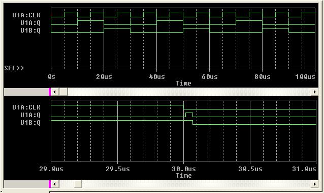
Note a glitch at 30us and delay times between signals.