ENEE 206
April 6, 2004
Laboratory 14 - Monostable and astable circuits
A. Lab Goals
- The main purpose of this lab is to introduce monostable and astable circuits.
- Another goal is to introduce the 555 timer chip, to understand how it works and to
learn about a few of its uses, including how it can be used to build a digital clock.
- We will also investigate a few other hybrid analog/digital monostabe and astable
circuits and characterize their performance.
- We will compare the operation of TTL and CMOS astable circuits.
B. Background Reading
- Read section 6.6 in Nelson Nagle (N/N) on 555 timers [or read section 11.15 in Mano (M)]. Also read
555 Timer Tutorial.
- Read the notes carefully because some of the astable circuits are not found in the
usual references.
- Make certain that you read the laboratory procedure ahead of time and answer the
Pre-lab questions.
C. Definitions
- Astable circuit - a circuit that has no stable states. A clock is an example of astable circuit.
- Monostable circuit - a circuit that has only one stable state. If an input occurs
that causes the circuit to transit to the unstable state, after some (fixed) period of time
the circuit will return to the stable state without any further changes to the input values.
A one-shot circuit is a monostabe circuit that gives one output pulse per trigger signal.
- Momentary switch - A switch that only has one steady-state position. The switch
contact is generally spring-loaded, so pushing the switch button changes the switch contact
position, but removing your finger brings the switch back to the origianl postion.
D. Laboratory Equipment
- There is no new equipment required for the Lab: Oscilloscope, DMMs, and LC meters will be
used in the course of the experiment.
E. New Hardware
- The 555 timing module is an integrated circuit that can be used for a large number of
applications, one of which is a simple clock.
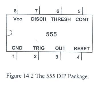
- The 555 comes in a DIP package with 4 pins on each side. The L555 or ICM7555 are CMOS
versions of the 555 timer and they have the same connections as the TTL version. Sometimes the
control pin (5) is called the bypass (BYP) pin.
- A simlified schematic of the 555 circuit is shown in Fig. 14.3 and a crude description
oif its operation follows.
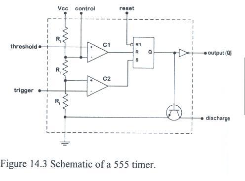
- At the center of the 555 is a set-reset flip-flop with a second reset, which is active
low and simply connected to the external reset (pin 4).
- The other reset input and the set input are active high and are connected to comparators
(C1, C2) which are essetially op-amps (see Chap. 16) without feedback elements.
- There are two inputs labeled plus (+) and minus (-) and one output. Whenever the plus
input is at a higher voltage level than the minus input, the output of the comparator is a logical
one. When the minus input is higher than the plus, the output is a logical zero.
- The input impedances of the comparators are very large, so the three equal resistors (Ri)
connected between VCC (pin 8) and ground (pin 1) function as a simple voltage divider
that provide 2VCC/3 to the minus terminal of the comparator connected to rest (C1) and
VCC/3 to the plus terminal of the comparator connected to set (C2).
- Note: this is only true when no connection is made to the control pin.
- Thus, whenever the threshold (pin 6) is greater that 2VCC/3, R will be
high and whenever the trigger (pin 2) is less than VCC/3, S will be high. Recall
that the output when R and S are both high is undefined, so that situation should be avoided.
- The output (pin 3) will be high after S has been high until R goes high. Only the
operation of one new component remains to be explained - the one between discharge (pin7) and
ground.
- This 3 terminal component is an NPN transistor and its operation is beyond the scope of
this course. The terminal connected to the discharge is called the collector; the one connected
to Qbar is the base, and the emitter is connected to ground.
- The transistor operation for this configuration is simple.
When the output Q is high,
the transistor base is at ground, the transistor is "off" and emitter-collector current flow is
zero (like an open switch).
When the output Q is low, the base is at a higher voltage, the
transistor is turned "on", and current flows from the collector to the emitter as if connected
by a short (like a closed switch).
The control connection (pin 5) provideds a means for altering
voltages across the divider resistors.
F. Circuit Analysis
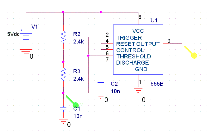
- To see how the 555 can be used to make a clock, consider the circuit in Fig. 14.4. There are
several things to notice.
- First, reset (R1) is connected to VCC, so the external reset is not used.
Neither is the external control used.
- The 0.01 mF capacitor will simply be charged up 2VCC/3
once the circuit is turned on and remain there.
- The threshold and trigger are tied together, so the pathological case S = R = 1 will
never occur.
- First assume the output is high. Then the transistor is off, the discharge pin is
essentially an open circuit, and the components attached to the threshold/trigger pins can be
modeled by the simple 1st order RC circuit shown in Fig. 14.5.
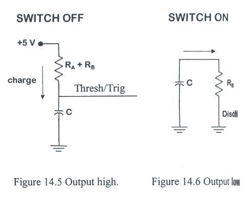
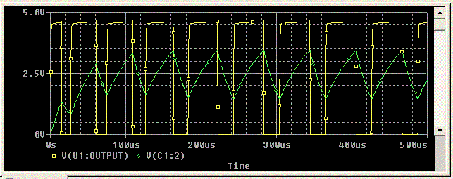
- Thus, the threshold voltage will start at some initial value and increase exponetially
with a time constant t1 = (RA + RB)C.
- This continues until the threshold voltage hits 2VCC/3. At that point, the
flip-flop is reset and the output goes low.
- This causes the transistor to turn on and the circuit connected to the trhreshold/trigger
pins now looks like the RC circuit shown in Fig. 14.6.
- Thus, the capacitaor voltage will discharge according to the formula
- VTh = (2VCC/3)e-t/t2,
where t2 = RBC.
- The discharge will coninue until the threshold/trigger voltage reaches VCC/3.
- At this time (toff = t2 ln2), the flip-flop
is set, the output goes high and we are back to the situation shown in Fig. 14.5. Thus we can write
the threshold voltage as
- VTh = VCC(1 - 2/3e-t/t1).
- Because this continues until VTh = 2/3 VCC, we find the on time to
be given by
- ton = t1ln2.
- Thus, total period is T = ton + toff =
(t1 + t2) ln2 =
(RA + 2RB)C ln2.
- The frequency of this clock is f = 1/[(RA + 2RB)C ln2] or
1.44/[(RA + 2RB)C].
- The frequency is in kHz if C is given in mF and the resistances
are in kW. The duty factor is
- ton/T = ton/(ton + toff) =
(RA + RB)/(RA + 2RB),
- which is always greater than 50% (setting RA = 0
would short out the supply when the output is low).
- If you want to see more details on the operation of this 555-based clock, go to Appendix B,
where the PSpice simulations results are displayed.
- The logic diagrams for 555-based monostable circuits are shown in Fig. 14.7.
There are only a few variations between the circuit in Fig. 14.7(a) and the clock circuit
of Fig. 14.4(a), yet the operation of the circuit changes significantly.
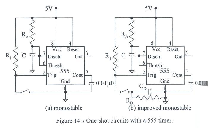
- The first difference is that RB is set to zero, so that the discharge
and threshold are shorted together.
- The trigger is disconnected from the threshold and tied to VCC via a
resistor R1.
- The resistance of R1 is not critical, but should be a few thousand ohms.
You must refer to Fig. 14.3 to understand how the circuit works.
- Assume temporarily that the output is zero. That means that the output complement is high,
so the transistor is on and the discharge is connected to ground.
- Thus the threshold is grounded, so the FF reset is zero. Likewise, the FF set is zero
because the trigger is at VCC. These are the settings for the stable state of the
circuit - the state which can be maintained indefinitely.
- Now consider the switch in the circuit. Actually, this switch should be a momentary
switch(not a DIP switch), so that the switch closes when you press a button, and the switch
automatically reopens when you release the button.
- When the switch is closed, the trigger pin rapidly changes to zero. The comparator C2
then goes high, so the set input goes to one and the output state chages to one.
- If the switch is then opened, the set goes low, but output remains high. Since the
output is high the transistor turns off and the discharge line "floats" with the threshold.
- That leaves us in the same situation shown in Fig. 14.5 with RB = 0.
Thus, the capacitor C charges up, and when it reaches a voltage of 2VCC/3, C1 goes high,
so the FF resets and we are back in the stable state with zero output.
- This explains why the circuit is called a monostable circuit
(sometimes it is also called a one-shot circuit).
- It will remain in the one state indefinitely, but it will remain in the other state only
for a short time that depends on RA and C. This assumes that the switch is released before
the circuit returns to its stagle state. What do you think happens if the switch is closed for
longer that that?
- The circuit in Fig 14.7(b) is designed to allow the switch to be connected for time
periods longer than the pulse length of the monostable. Even if the switch is connected, CD
will charge up, and as soon as the voltage in CD exceeds VCC/3, the set
line will go to zero.
- The additional resistors and capacitor must be chosen so that the set line goes to
zero before the reset line goes high.
- If the pulse length is very short, you should probably debounce the switch so that you
don't get more than one pulse unexpectedly.
- In Fig. 14.8 we show a number of different astable circuits which utilize simple
gates to generate a clock signal.
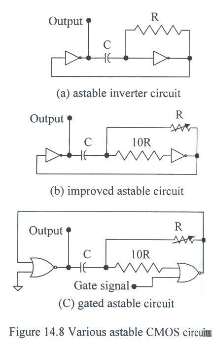
- Consider the simple two inverter circuit shown in Fig. 14.8(a). Assume first that there is
no charge on the capacitor and that the output is low.
- Then the output of the right-most inverter is positive and the inputs and outputs of
both chips are self-consistent.
- Because the CMOS chips have very large input impedances, the RC combination looks like
the situation in Fig. 14.5 and the capacitor starts to charge.
- Because CMOS circuits tend to change states at half the supply voltage
(i.e., a logical zero is 0 < Vin < VCC/2 and a logical one is
VCC/2 < V < VCC, the right-most inverter output will transit to zero as
soon as the capacitor voltage exceeds VCC/2.
- This will force the output of the left-most inverter high.
- We know that the voltage on a capacitor is continuous, so the voltage difference
from the left side of the capacitor to the right side of the capacitor must remain VCC/2,
- Since the left side of the capacitor jumps from zero to VCC, the right
side of the capacitor must jump to 3VCC/2. This means that there is a voltage difference
across the resistor of 3VCC/2, so the capacitor begins to discharge through the resistor.
- Current would flow in principle until the resistor voltage goes to zero, but again the
right-most inverter will flip states once the resistor voltage goes below VCC/2.
- Just before the inverter flips, the voltage on the left side of the dcapacitor is still
VCC, while the voltage on the right side is VCC/2, so the voltage difference
from left to right is -VCC/2.
- When the right inverter goes high, the left inverter goes to zero, and the voltage on
the right side of the capacirtor gets pulled to -VCC/2.
- Thus, the resistor starts to charge the capacitor towards VCC. (Once again
there is a 3VCC/2 voltage difference across the resistor.)
- This cycle then repeats to give us our square wave output. The capacitor voltage is
always attempting to swing by 3VCC/2, but it only makes it 2/3 of the way.
- Following an analysis similar to what we did for the 555 timer circuit, we can find
that the period of a full oscillation is T = 2RC ln3. The frequency is then approximately
f = 1/(2.2RC).
- There is a problem with the first circuit that has to do with the way that CMOS
chips are constructed. The details are beyond the scope of this course, but basically it
involves diodes that are part of the CMOS chip to protect it from incorrect voltages.
- These diodes can tend to round the output pulse, cause the frequency do depend on
VCC, and possibly yield an asymmetric output pulse (not a 50% duty factor).
- The additional resistor shown in Fig. 14.8(b) eliminates these problems. Since the
input impedances of the CMOS chips are quite large, this resistor doesn't significantly effect
ideal operation of the circuit.
- In general, the new resistor is made large compared to the original rsistor, but
in the lab you can play with this value to produce the best performance.
- The variable resistor is shown as a way to vary the frequency.
- The circuit in Fig. 14.8(b) shows a gated clock. The left-most NOR gate simply
functions as an inverter.
- When the gate signal is high, the output is locked high. When the gate is moved low,
the right most NOR functions as an inverter and the circuit operates exactly as the clock circuit
in Fig. 14.8(b).
- Note that these circuits operate with a 50% duty cycle, which is usually what you
want with a clock.
- Can you figure out how to use two diodes and two resistors to make a clock with a
duty cycle different from 50% (or two diodes and one potentiometer)?
- Why do we talk about CMOS circuits and not TTL circuits? You should be able to think
of at least 2 differences between CMOS and TTL technology that would affect the analysis here if we
tried to apply it to TTL technology.
G. Helpful Hints
- You need to run the oscilloscope in single-shot mode for the one-shot circuit.
- In this lab we will run CMOS chips at voltages well above 5 V. Make certain that you
do not run TTL chips at any voltage except 5 V. If a chip gets hot/ smells funny / is smoking(!)
it is probabley not connected properly or the voltage is wrong. Turn off the power supply
immediately and check that the chips are inserted properly (not upside down, shorted out by
the breadboard, etc.) and that the wires are connected properly. Note that connecting the
outputs of two different components together is a frequent cause of circuit malfunction.
If there are no wiring mistakes, remove the power leads to the circuit and check the power
supply voltage.
- Try to arrange your components on the breadboard in a similar arrangement as on
the wiring diagram.
Laboratory 14 Description - Monostable and astable circuits
Objective:
- In this lab we will use a 555 timer chip to build a digital clock and a one-shot. We
will also build simple clocks from both TTL and CMOS chips and compare their performance.
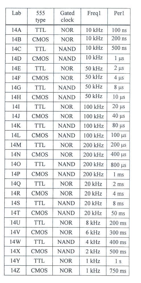
- In the lecture you will be told to do one of the following labs: 14A - 14Z.
Look in the table to discover the components and frequencies specific to your lab.
Do Lab 14x, where the x corresponds to your group(station).
Available Hardware:
Digital component boxes - see Appendix G, and momentary switches.
Pre-lab preparation:
Unless otherwise stated, asssume for the following circuits that there is a simple resitive load
R and and AC source with an amplitude of 5 V(rms).
Part I - 555 timer clock circuit
- ....
- ....
Part II - 555 timer one-shot circuit
- ....
Part III - Gated clock
- ....
- ....
Experimental Procedure:
During this experiment, be certain that you:
- Ask the TA questions regarding any procedures about which you are uncertain.
- Turn off all power supplies any time that you make any change to the circuit.
- Arrange your circuit components neatly and in a logical order.
- Compare your breadboards carefully with your circuit diagrams before applying power to the circuit.
- Note: ONLY for step 6 below use the function generator as the source. For all other srtewps, use the 60 Hz vriable transformer in the black bos!!! Set rhe rms voltage of the ad source to t V.
- Complete the following tasks:
Part I - 555 timer clock circuit
- ....
- ....
Part II - 555 timer one-shot circuit
- ....
Part III - CMOS gated clock circuit
- ....
- ....
- ....
Part IV - TTL gated clock circuit
- ....
Post-lab analysis:
Generate a lab report following the sample report available in Appendix A. Mention any
difficulties encountered during the lab. Describe any results that were unexpected and try
to account for the origin of these results(i.e. explain what happened). In ADDITION, answer
the following questions:
Part I - 555 timer clock circuit
- ....
- ....
- ....
- ....
- ....
Part II - 555 timer one-shot circuit
- ....
- ....
Part III - CMOS gated clock
- ....
- ....
- ....
- ....
Part IV - TTL gated clock
- ....
Part I and III - Answer the question if you performed both experimental parts.
- ....
Laboratory 8 Pre-lab Questions - Rectifier circuits
- ....
- ....
- ....
- ....
- ....
- ....
- ....