B. Background Reading
C. Definitions
- A/D Converter - a device that converts a analog signal to a digital signal at certain time intervals
D. Laboratory Equipment
E. New Hardware
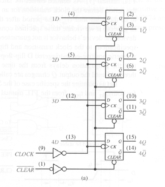
Positive-edge triggered D flip-flop 74175.
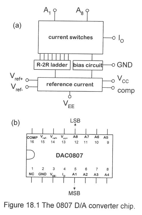
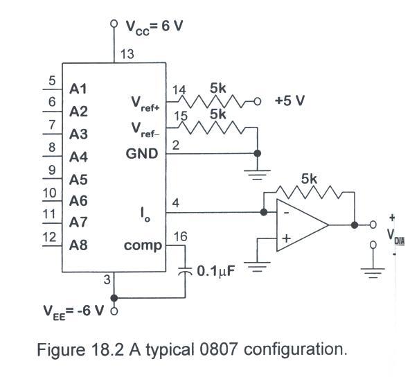
F. Circuit Analysis
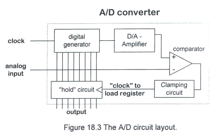
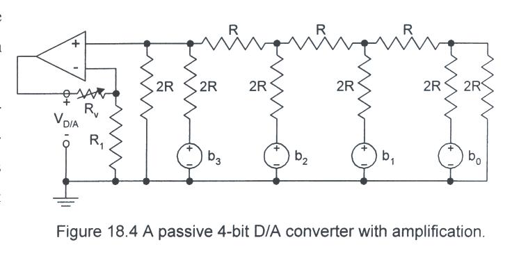
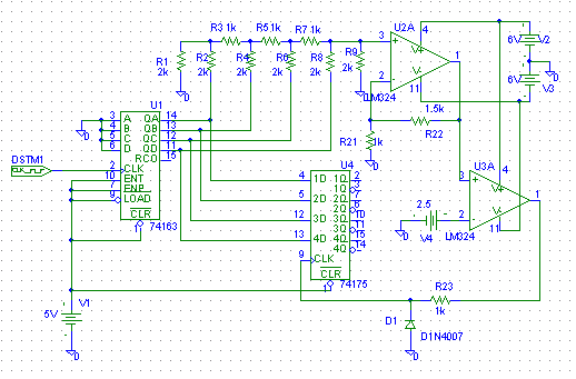
The non-inverting amplifier is connected to the passive D/A "output" to achieve the desired maximum output level and to provide isolation for the passive load. An alternative configuration for the D/A connverter would involve using the multiple source inverting amplifier described in the notes for Lab 16.
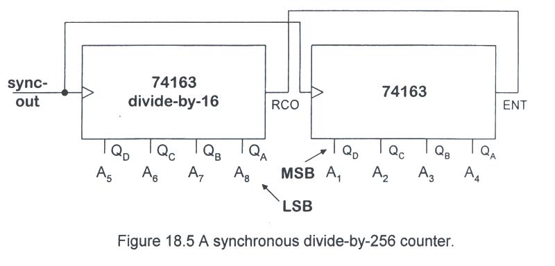
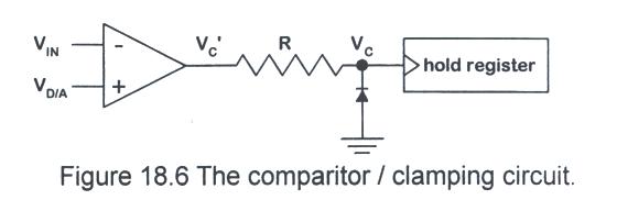
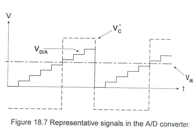
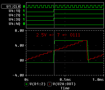
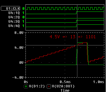
PSpice Simulation of 4-bit A/D Converter
G. Helpful Hints
Because this lab report is turned in at the end of the lab, be absolutely certain that you have read entire lab handout carfully, so that you can finish everything on time.- You may want to insert a buffer (2x7404 or 7407) between the compararor circuit ourput to the quad flip-flop.
Laboratory 18 Description - Analog-to-digital Converters
Objective:
Available Hardware:
Pre-lab preparation:
- Design a 4-bit D/A converter using a resistor ladder. Assume that the voltage for a logical one is between 3.3 and 5 V and design an amplifier with a variable gain (via potentiometer) so that an input of "1111" results in an output volrage of 5 V and an input of "0000" results in a voltage of 0 V. Assume the op-amp supplies are +/- 6 V.
- Draw the wiring diagrm.
- Use PSpice to simulate the circuit. Use a divide-by-16 couter to drive the four inputs. Use a clock frequency of 1 kHz. Plot the analog inputs, the intermediate output signal, and the final output signal simultaneously.
Part II - 4-bit A/D converter
- Design a 4-bit A/D converter that uses the D/A converter from Part I. Use a counter to generate the digital numbers, a register (or set of flip flops) to hold the result, and a comparator to generate the clock pulse. Note: the compatator output must be between -1 V and +6 V. Use a potentiometer attached to +5 V and ground to generate the input analog signal.
- Draw the wiring diagram.
Part III - 7-bit D/A converter
- Look up the data sheet for the DAC0807 D/A chip via the web page. Modify the "typical application" figure so that an input of "1111111" results in an output of 5 V and an input of "0000000" resultls in an outout of 0 V.
- Draw the wiring diagram.
Part IV - 7-bit A/D converter
- Design a 7-bit A/D converter that uses the DAC0807 D/A chip.
- Draw the wiring diagram. See a sample schematic diagram.
Part I - 4-bit D/A converter
Experimental Procedure:
During this experiment, be certain that you:
- Ask the TA questions regarding any procedures about which you are uncertain.
- Turn off all power supplies any time that you make any change to the circuit.
- Arrange your circuit components neatly and in a logical order.
- Compare your breadboards carefully with your circuit diagrams before applying power to the circuit.
- Below, insert for "m" the last digit of the current year, i.e. if the year is 2003, then m = 3.
- Below, use Vino = (1.85 + m/5) Volts, i.e. if the year is 2003, then Vino = 2.45 V.
- Complete the following tasks:
- Build the 4-bit D/A converter circuit. Drive the circuit with a 4-bit binary counter. Set the clock frequency from the Sync Out of the function generator to 1 kHz.
- Make a plot which shows the output voltage from the D/A converter and the clock signal used to drive the counter.
Part II - 4-bit A/D converter
- Build the 4-bit A/D converter circuit.
- Adjust the analog input signal to Vino.
- Attach a copy of the oscilloscope plot which has the D/A output, the comparator output, and the analog input signal.
- Attach a copy of a digital logic analyzer output which shows the output from the counter and the output from the A/D.
Part III - 7-bit A/D converter
- Build the 7-bit A/D converter circuit. Set the clock frequency to 16 kHz.
- Adjust the analog input signal to Vino.
- Attach a copy of the oscilloscope plot which has the D/A output, the comparator ooutput, and analog input signal.
- Attach a copy of a digital logic analyzer output which shows the output from the counter and the output from the A/D.
Part I - 4-bit D/A converter
Post-lab analysis:
If this is not your final experiment, perform the post-lab analysis as usual and turn in your lab report the following week.
- What are the ACTUAL values of the resistances used in your D/A converter? How do the actual values effect the analog output voltages of the S/A?
- How might one improve the performance of the D/A converter?
- How do the measured results compare with the PSpice simulations?
Part II - 4-bit A/D converter
- Given a digital output of m + 3, what is the estimate of the analog voltage input and what is the uncertainty? Get your answer from the measurements and not from the ideal model.
- Can you get the comparator output to "malfunction"? If so how?
- What are the comparator output voltages for both cases (when the analog signal is larger than and smaller than the D/A output)?
Part III - 7-bit A/D converter
- What has the better resolution, the DAC0807 or the oscilloscope screen? Justify (quantify) your answer.
- What are the digital outputs (according to the DLA) that correspond to the input voltages listed to the right? Vin = 0.1 V, 1.0 V, 1.6 V, 2.8 V, 3.3 V, 4.1 V, 4.9 V.
Part II or III - A/D converters
- Besides the D/A converter, how might one improve the performance of the A/D converter?
Part II and III - A/D converters
- Compare the performance of the two D/A converters.
Part I - 4-bit D/A converter
|
|