ENEE 206
April 27, 2004
Laboratory 17 - Passive and Active Filter Design
A. Lab Goals
For this lab you will design, scale, construct, and test active and/or passive filter circuits. You will compare the frequency performance of a number of different filters.
B. Background Reading
Read sections 9.3 - 9.7 in (M/L) on frequency response and filter circuits.
C. Definitions
- Active Filter - filters constructed with op-amps. Potentially can exhibit power gain.
- Band Notch Filter - A circuit that rejects a range of frequency signals to a circuit but allows low and high frequency signals to pass through with a fairly constant gain.
- Band Pass Filter - A circuit that allows a range of frequency signals to pass through a circuit but attenuates low and high frequency signals.
- Butterworth Filter - A type of filter that is "maximally flat", i.e. as many derivatives of the magnitude of the transfer function as possible are equal to zero at some specified frequency.
- Corner Frequency - The frequency where the power in the output signal is 50% of the output power in the passband. This is also known as the 3dB freqency and the breakpoint frequency.
- Filter Circuit - A circuit that conditions an input signal, usually by allowing only a range of frequencies to pass through the circuit to the output. The purpose of a filter is often to separate a desired signal from undesired signals (e.g. noise).
- High Pass filter - A circuit that allows high frequency signals to pass through a circuit buyt attenuates low frequency signals.
- Low Pass Filter - A circuit that allows low frequency signals to pass through a circuit either unattenuated or with a fairly constant gain (or loss) but attenuates high frequency signals.
- Normalized filter Circuit - A circuit whose parameters are adjusted so that the corner frequency is 1 radian/sec and the output impedance is 1 W.
- Passband - The range of frequencies that passes through a filter relatively unattenated (or at least fairly niformly).
- Passiv Filter - filters constructed without op-amps. Typically have an insertion loss of 6 dB.
- Roll Off - The rate (in dB/decade) that the power in a signal is attenuated outside of the passband as a function of frequency.
D. Laboratory Equipment
No new equipment will be used in this lab.
E. New Hardware
No new hardware will be used for this lab.
F. Circuit Analysis
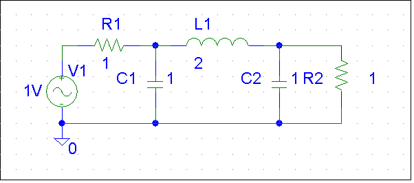
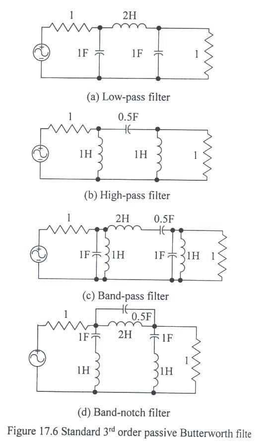
In this lab we will analyze two very different circuits which are designed to accomplish the same task. The first circuit has only passive components (R, L, and C) and is shown in Fig. 17.1a.
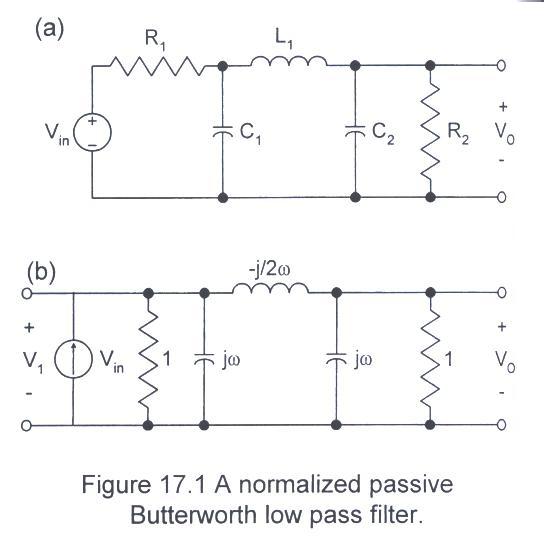 At low frequencies, capacitors act as open circuits and inductors act as short circuits, so the circuit is a simple resitive divider at low frequencies with
V0/Vin = R2/(R2 + R1).
At high frequencies, inductors have high impedance and capacitors have low impedance. Because the capacitors in Fig. 17.1a are in parallel with the output (sort of) and the inductor is in series with the output, all three components tend to reduce the output signal at high frequency. Therefore, this circuit is called a 3rd-order low pass filter. The details of the frequency response depend on the particular values of the components.
At low frequencies, capacitors act as open circuits and inductors act as short circuits, so the circuit is a simple resitive divider at low frequencies with
V0/Vin = R2/(R2 + R1).
At high frequencies, inductors have high impedance and capacitors have low impedance. Because the capacitors in Fig. 17.1a are in parallel with the output (sort of) and the inductor is in series with the output, all three components tend to reduce the output signal at high frequency. Therefore, this circuit is called a 3rd-order low pass filter. The details of the frequency response depend on the particular values of the components.
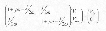
We will use general nodal analysis to model a normalized filter circuit where we take the values in Fig. 17.1a to be C1 = C2 = 1F, R1 = R2 = 1 W, and L1 = 2H. The resultant admittances are indicated in Fig. 17.1b, where we have also transformed the nonideal voltage source into a nonideal current source. There are three nodes, so we take the lowest node to be ground and find the nodal equations in matrix form to be:
 which can be inverted to find
 or
Vout = Vin/2jw/[(1 + jw - j/2w)2 + (j/2w)3],
or simply
Vout/Vin = 1/2/
[1 + 2jw + 2(jw)2 + (jw)3].
The magnitude of the transfer function is
|Vout/Vin| = 1/2/[(1 - 2w2)2 + w2(2 - w2)2]1/2 = 1/2/(1 + w6)1/2
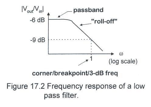
after a little algebra. This filter is known as a (3rd-order) Butterworth filter. It is also called a "maximally-flat" low-pass filter because the first 2n-1(n=3) derivatives of the transfer function are zero at w = 0. A picture of the transfer function magnitude, or gain, is shown in Fig. 17.2 as a function of frequency.
or
Vout = Vin/2jw/[(1 + jw - j/2w)2 + (j/2w)3],
or simply
Vout/Vin = 1/2/
[1 + 2jw + 2(jw)2 + (jw)3].
The magnitude of the transfer function is
|Vout/Vin| = 1/2/[(1 - 2w2)2 + w2(2 - w2)2]1/2 = 1/2/(1 + w6)1/2
after a little algebra. This filter is known as a (3rd-order) Butterworth filter. It is also called a "maximally-flat" low-pass filter because the first 2n-1(n=3) derivatives of the transfer function are zero at w = 0. A picture of the transfer function magnitude, or gain, is shown in Fig. 17.2 as a function of frequency.
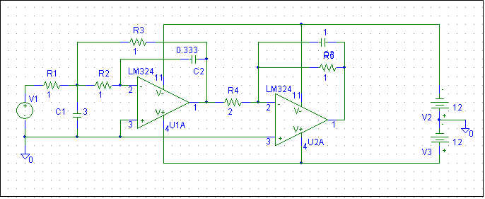
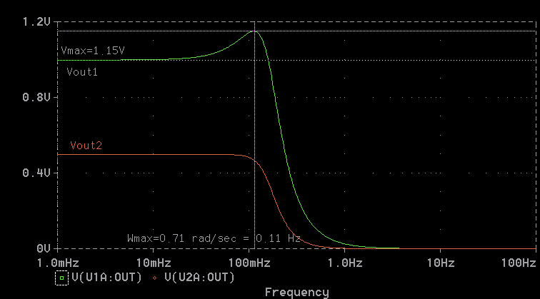
PSpice Simulation
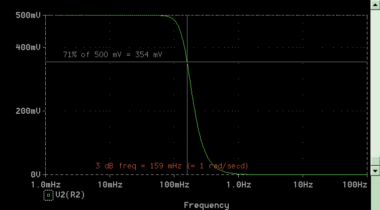
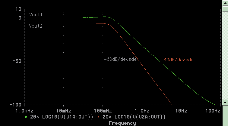
 The maximum voltage gain is 1/2 at low frequencies and the corresponding power gain is 1/4 since for a resitive load, the power is proportional to the foltage squared. The frequency range where the gain is nearly flat is called the pass band. The corner frequency where the gain has decreased by the square root of 2 is w = 1 rad/sec. Above this frequency the output voltage "falls off" from the maximum value by 3 orders of magnitude for every decade increase in frquency.
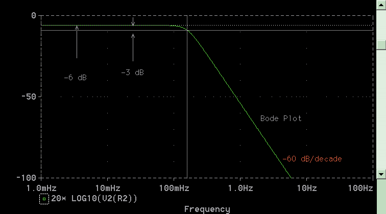
It is often useful to take the logarithm of the transfer function:
|Vout/Vin|(dB) = 20 log10|Vout/Vin|
= 20 log10(1/2) - 20 log10(1 + w6)1/2
= -6 -10 log10(1 + w6)
For low frquencies
|Vout/Vin| = -6 dB.
This value is called the insertion loss. For high frequencies (w >> 1),
|Vout/Vin| ~ -6 - 60 log10(w) dB
Thus, we say the roll-off is approximately 60 dB/decade. The roll-off of a slow pass filter is always 20 dB/decade times the order of the filter (3 in this case).
Typically, a filter that has a corner frequency of 1 rad/sec and is used with a load impedance of 1 W is not very interesting. But the process of filter synthesis via frequency and impedance denormalization can be used to transform this design into one with a desirable corner frequency and load impedance. This is nice, because every time you need to design a filter for a new frequency or impedance, you don't need to start from scratch. If the required load impedance is RL and the required corner frequency is w0, simply take any values of R, L, and C that you find in the normalized circuit and replace them with R', L', and C', respectively, according to the following formulas:
R' = R x RL
L' = L x RL/w0
C' = C/(RL x w0).
As a concrete example, say we want to have a load impedance of 51 W and a corner frequency of 3.45 kHz for our 3rd-order low pass filter, we weuld replace both resistances with 51 W (the resistor on the right is the load resistor, by the way). The 2 H inductor would be repladed by
L' = 2 x 51/(2p x 3.45 x 103) = 4.7 mH
and the capacitors would be
C' = 1/(51 x 2p x 3.45 x 103) = 0.9 mF
That's all there is to scaling!
Consider now the active filter shown in Fig. 17.3.
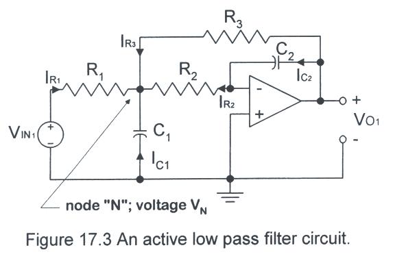 To solve for the voltage transfer function, we write KCL at node N:
IR1 + IR2 + IR3 + IC1 = 0
Because the inverting terminal is at vertual ground, we can easily write those four currents in terms of Vin1, V01, and VN:
IR1 = (Vin - VN)/R1,
IR1 = -VN/R2
To solve for the voltage transfer function, we write KCL at node N:
IR1 + IR2 + IR3 + IC1 = 0
Because the inverting terminal is at vertual ground, we can easily write those four currents in terms of Vin1, V01, and VN:
IR1 = (Vin - VN)/R1,
IR1 = -VN/R2
IR3 = (VO1 - VN)/R3,
IC1 = -sC1VN
But the current into the inverting terminal is zero, so
-VN/R2 = IR2 = IC2 = sC2V01
or
VN = -sR2C2V01
Therefore, we can comgine all the equations and rearrange the terms to get the voltage transfer function:
Vo1/Vin1 = -1/[R1/R3 + sC2R2R1(1/R1 + 1/R2 + 1/R3 + sC1)]
= (-1)/(R1R2C1C2)/[s2 + s(1/R1 + 1/R2 + 1/R3)/C1 + 1/(R2R3C1C2)].
To get our normalized filter, we are going to choose R1 = R2 = R3 = 1 W, C1 = 3 F, and C2 = 1/3 F. Plugging these values in yields:
Vo1/Vin1 = -1/(s2 + s + 1) = -1/[(jw)2 + jw + 1]
so
|Vo1/Vin1| = 1/[(1 - w2)2 + w2]1/2 = 1/(1 - w2 + w4)1/2.
A plot of the magnitude of this transfer function is given in Fig. 17.4.
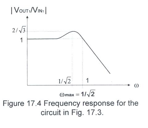 Note that the response is not maximally flat. In fact, the response has a maximum that can be found bve setting the derivative of the transfer function to zwro. The resut is
wmax = 1/21/2
and
|Vout/Vin(wmax) = 2/31/2.
Finding the gain in dB yields:
|Vo1/Vin1|(dB) = -20 log101/(1 - w2 + w4)1/2 = -10 log10(1 - w2 + w4).
For high frquencies
|Vo1/Vin1|(dB) = -40 log10w,
so the roll off is 40 dB/decade and this is a second order low-pass circuit. This is not surprising vecause there are two capacitors, one in parallel with the input. To scale this result to an unnormalized frequency and impedance, you use the same scaling rules which were spelled out for passive filters.
Note that the response is not maximally flat. In fact, the response has a maximum that can be found bve setting the derivative of the transfer function to zwro. The resut is
wmax = 1/21/2
and
|Vout/Vin(wmax) = 2/31/2.
Finding the gain in dB yields:
|Vo1/Vin1|(dB) = -20 log101/(1 - w2 + w4)1/2 = -10 log10(1 - w2 + w4).
For high frquencies
|Vo1/Vin1|(dB) = -40 log10w,
so the roll off is 40 dB/decade and this is a second order low-pass circuit. This is not surprising vecause there are two capacitors, one in parallel with the input. To scale this result to an unnormalized frequency and impedance, you use the same scaling rules which were spelled out for passive filters.
To arrive at 3rd-order Butterworth filter, we are going to cascade another op-amp stage on the end of the circuit we just analyzed. This circuit is shown in Fig. 17.5.
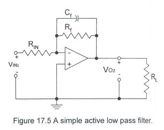 Recalling the general formula that we derived for inverting amplifiers, we can quickly get the voltage transfoer function for this circuit:
Vo2/Vin2 = -Zf/Zi = -(Rf/(sCf)/(Rf + 1/sCf)/Rin = -Rf/Rin/(1 + sRfCf).
Our normalized filter comes from selecting Df - 1 F, Rf = 1 W, and Rin = 2 W, so
Vo2/Vin2 = -1/2/(1 + s) = -1/2/(1 + jw)
The net transfer function when these two op-amp circuits are cascaded in seried is:
Vo2/Vin1 = (Vo2/Vin2)(Vin2/Vin1) = (-1/2)/(1 + w) {-1/[1 + jw + (jw)2]}
or
Vo2/Vin1 = (1/2)/[1 - 2w2 + jw2 + jw(2 - w2)2].
This is the same expression we had for the passive circuit, so once again the magnitude of the gain is
|Vo2/Vin1| = 1/2/(1 + w6)1/2.
Recalling the general formula that we derived for inverting amplifiers, we can quickly get the voltage transfoer function for this circuit:
Vo2/Vin2 = -Zf/Zi = -(Rf/(sCf)/(Rf + 1/sCf)/Rin = -Rf/Rin/(1 + sRfCf).
Our normalized filter comes from selecting Df - 1 F, Rf = 1 W, and Rin = 2 W, so
Vo2/Vin2 = -1/2/(1 + s) = -1/2/(1 + jw)
The net transfer function when these two op-amp circuits are cascaded in seried is:
Vo2/Vin1 = (Vo2/Vin2)(Vin2/Vin1) = (-1/2)/(1 + w) {-1/[1 + jw + (jw)2]}
or
Vo2/Vin1 = (1/2)/[1 - 2w2 + jw2 + jw(2 - w2)2].
This is the same expression we had for the passive circuit, so once again the magnitude of the gain is
|Vo2/Vin1| = 1/2/(1 + w6)1/2.
PSpice Simulation
 The disadvantage of the active filter is that it requires op-amps, which in turn require two
power supplies in order to function properly. The passive filter can be constructed, placed in
a tiney box with appropriate connectors, and inserted in a signal line and function poperly
without any concerns or maintenance.
The disadvantage of the active filter is that it requires op-amps, which in turn require two
power supplies in order to function properly. The passive filter can be constructed, placed in
a tiney box with appropriate connectors, and inserted in a signal line and function poperly
without any concerns or maintenance.
On the other hand, the active circuit has many advantages. First, it requires no indudctors,
which are often heavy, not readily availagle off-the-shelf in a variety of values, and can
interact with other neaby inductors. Also, the gain is fairly independent of the load impedance.
This is not true for passive circuits as you can see ;by reanalyzing the circuit in Fig. 17.1
with R2 =/ R1. Finally, active filter can actually have insertion gain,
rather than insertion loss, by choosing proper values for the resistors.
The scaling laws that we presented for passive filters, to convert normalized designs to
designs for realistic frequencies and realistic loads, apply equally to acrtive filters.
G. Helpful Hints
- Build and test the active filter in stages.
Laboratory 11 Description - Passive and Active Filtler Designs
Objective:
To compare the performance of active and passive 3rd-order Butterworth filters.
Available Hardware:
Analog component boxes - see Appendix G.
Incuctors: 4.7 mH, 10 mH, 20 mH, 50 mH.
All of you will do the lab 17A in the Table 17.1. All labs will require the design,
analysis, and comparison of tow different filter circuits. The parameters are given in the table
below. Unless it is stated otherwise in class, all passive filters are Butterworth filters.
The corner/ceter frequency of each filter will be the same. The post-lab questions are also all
the same, even though the answers may vary widely for the different types of op-amps. It is the
students responsibility to read the questions carefully and give a detailed, thoughtful answer
to each question as it relates to thier two circuits.
Pre-lab preparation:
For each filter, the order of the filter is given in Table 17.1: 2nd = second order ...etc.
Table 17.2 contains the abbreviations for the other characteristics dictated in the first table.
Below, when the instructions talk about the corner/ecenter frequency, "corner" refers to LP and
HP filters and "center" refers to BP and BN.
Part I - First Filter
- Design Filter1 as indicated in lthe table with a corner/center frequency of about Freq:____
and a load resistance of about RL:_____.
- Draw the circuit diagram.
- Use PSpice to simulate the circuit performance. Plot the output voltage over a suitable range
of frequenciies. Plot both the magnitude and phase of the output. Assume the input voltage is
2 V peak-peak.
- Double the output resistance in the circuit and repeat the simulations.
Part II - Second Filter
- Design Filter2 as indicated in the table with the same corner/center frequency of about
Freq:____ and the the same load resistance of about RL:_____.
- Draw the circuit diagram.
- Use PS;pice to simulate the circuit performance. Plot the output voltae overt a suitable range
of frequencires. Plot both the magnitude and phase of the output. Assume the input voltage is
2 V peak-peak.
- Double the output resistance in the circuit and repeat the simu;ations.
Experimental Procedure:
This is the final experiment for the semester, use the "lab analysis" secton on page 240 to record your data.
If this not your final lab,...
During this experiment, be certain that you:
- Ask the TA questions regarding any procedures about which you are uncertain.
- Turn off all power supplies any time that you make any change to the circuit.
- Arrange your circuit components neatly and in a logical order.
- Compare your breadboards carefully with your circuit diagrams before applying power to the
circuit.
- Use 12 V (plus and minus) for the op-amp power.
- Complete the following tasks:
Part I - First Filter
- Construct the first filter circuit(Filter1). Set the input voltage to 10 V peak-peak.
- Measure the relative magnitude and phase of the output voltage from 100 Hz to 1 MHz (use at
least 4 points/decade). Find the 3 dB point and plot the input and output voltages.
- Double the load resistance and repeat the previous measurement.
Part II - Second Filter
- Construct the second filter circuit(Filter2). Set the input voltage to 10 V peak-peak.
- Measure the relative magnitude and phase of the output voltage from 100 Hz to 1 MHz
(use at least 4 points/decade). Find the experimental 3-dB point and plot the input and ooutput voltages.
- Double the load resstance and repeat the previous measurement.
Post-lab analysis:
This is your final lab of this semester, you can skip over this section, answer only the
summation questions in the "lab analysis" section on page 244 and hand in the completed section
at the end of the lab period. Remember to make two plots of all your results.
If this is not your final experiment, .....