ENEE 206
Feburuary 10, 2004
Laboratory 3 - Switching Circuits and Digital Logic Analysers
A. Lab Goals
- The main point of this lab is to learn the capabilities and master their operation of a
Digital Logic Analyzer (DLA) when used as a timing analyzer.
- Other goals include the design
of a minimal swiching circuit, effective testing of all possible input combinations, and
the ability to identify gliches and measure time delays.
B. Background Reading
- Read "Feeling Comfortable with Logic Analyzers" in Appencix E in this manual.
- Also read Appendix F on the procedure for using the DLA.
- Read about synchronous counters
(eg., Section 7.3.1 in N/N or section 7.5 in M).
- Revieww switching circuits (Chapter 2 in N/N or Chapter 3 in M).
C. Definitions
- SOP - Sum Of Products: a two-level realization of a switching circuit where
the first level consists of AND(NAND) gates and the final level consists of OR (NAND) gate.
- POS - Product Of Sums: a two-level realization of a switching circuit where
the first level consists of OR(NOR) gates and the final level consists of AND(NOR) gate.
- Pod (of wires) - a set of 16 probe wires connected to the same input cable for DLA.
D. Lab Equipment
The Digital Logic Analyzer(DLA) is a powerful piece of test equipment and we will only
learn to use a few of its features in the course.
E. New Hardware
- Four new TTL chips:
- 7410 - 3 three-input NAND
- 7420 - 2 four-input NAND
- 7425 - 2 four-input NOR, each with a "strobe".
- 74163 - synchronous 4-bit(binary) counter
F. Circuit Analysis
- For this lab, you are asked to realize a switching circuit with four inputs.
- To test all combinations of the inputs, you can use the outputs of the synchronous counter.
- You may need to design both SOP and POS forms with as few chips as possible.
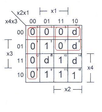
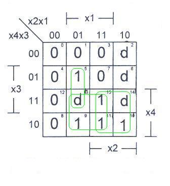
- Consider the switching function
f(x4,x3,x2,x1) = m(5, 9, 10, 11, 15) + d(2, 6, 13, 14),
shown in Fig. 3.3 along with a minimal covering.
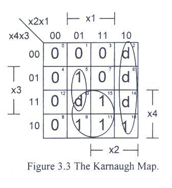
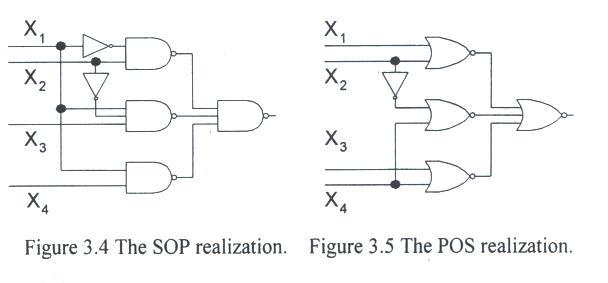
- The SOP result is f = X1X4 + X2X'1 + X'2X1X3
and
f' = X'1X'2 + X2X'4 + X'3X'4
- the POS result is f = (X1 + X2)(X'2 + X4)(X3 + X4).
- The NAND and NOR implementatations are shown in Fig. 3.4 and Fig. 3.5, respectively.
- How many chips are required?
- The SOP requires
- 2/6 of a 7404(NOT)
- 2/4 of a 7400(2-input NAND) and
- 2/3 of a 7410(3-input NAND).
- The POS reqires the same number of chips, but one less gate:
- 1/6 of a 7404,
- 3/4 of a 7402 and
- 1/3 pf a 7427.
- The SOP implementation has a potential problem with gliches.
- For example,
- if the current input X4X3X2X1 = 1011 then the output is one.
- If X1 goes to zero (X4X3X2X1 = 1010),
the output should remain at one, but a glitch may develop due to the delay through the upper inverter in Fig. 3.4.
- The realization f = X1X4 + X2X4 + X'2X1X3
will avoid this problem.
G. Helpful Hints
Read 1 through 4.
Laboratory 3 Description - Swithcing Circuits and Digital Logic Analyzers
Objective:
- To learn to use a Digital Logic Analyzer as a timing analyzer and
- to build and test SOP and POS realization of various four-variable switching
functions.
- To identify glitches and other non-ideal features.
Available Hardware:
- Digital component boxes - see Appencix G.
- In class, you will be told to do one of the following labs: 3A - 3R.
- Look at the table on page 43 for the components and switching function
f(X4, X3, X2, X1) that correspond to your lab.
Pre-lab preparation:
Part I - SOP Design
- Design a minimum SOP realization of f(X4, X3,X2,X1) using only TTL NAND gates.
- Draw the logic diagram and wiring diagram for the circuit.
- Use PSpice to simulate the SOP circuit and plot the output and the variable signals as a function of time
when you use a 74163 to generate the input signals.
Part II - POS Design
- Design a minimum POS realization of f(X4, X3, X2 X1)
using only TTL NOR gates.
- Draw the logic diagram and wiring diagram fot the circuit.
- Use PSpice to simulate the POS circuit and plot the output and the variable signals as a function of time
when you use a 74163 to generate the input signals.
See sample logic diagrams,
sample wiring diagram, and
sample output plots.
Part III - CMOS POS Design
- Draw the wiring diagram for the POS circuit using CMOS technology.
Part IV - CMOS SOP Design
- Draw the wiring diagram for the SOP circuit using CMOS technology.
Experimental Procedure:
During this experiment, be certain that you:
- Bring floppy disks(3 1/2) with you to the lab to store your traces.
- Ask the TA questions regarding any procedures about which you are uncertain.
- Turn off all power supplies any time that you make any change to the circuit.
- DO NOT apply more than 5V to the circuit at any time.
- Arrange your circuit components neatly and in a logical order.
- Compare your breadboards carefully with your circuit diagrams before applying power to the circuit.
- Complete the following tasks:
Part I - Input variable generation
- Use a 74163 synchronous divide-by-16 cunter to provide the variables to test your circuit.
Disable the load, clear, and hold(not enabled) features of the counter.
- Use the Sync Out" connector of the sweep generator, set to 20 kHz, to provide the clock input to the 74163.
- Use the oscilloscope to plot the clock and counter outputs simultaneously.
- Trigger off the clock, and split the oscilloscope screen into four sections,
- displaying one trace in each section.
- Measure the delay for each of the outputs(see page 19 for a definition).
Part II - Switching circuit construction
- Construct the switching circuit on your breadboard.
- Use the oscilloscope to plot the clock and output pulse. You may have trouble achieving a stable trigger.
One poosibility is to set the trigger to: triggered, delay, qualify on state, trigger on count 11.
Set the clock number to correspond to the probe channe connecgted to the output signal and adjust the delay to place
the zero output at the leftmost part of the screen. Plot the result.
- Measure the time delay bewtween the clock and the output signal, as well as the delays between the clock and
the intermediate switching circuit signals.
Part III - Digital logic analyzer
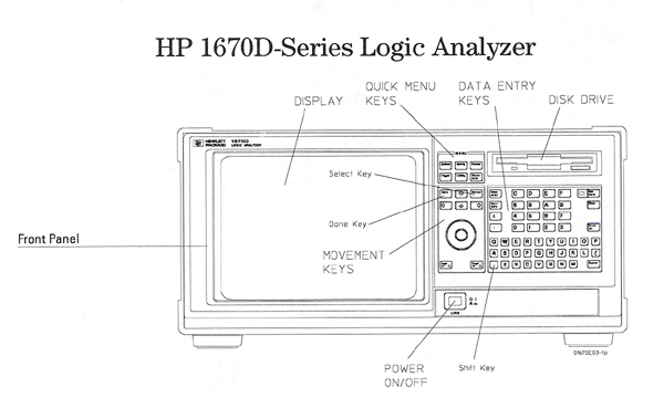
- Following the steps outlined in Appendix F, use the digital logic analyzer to plot the output of the circuit,
the four input variables, the output signal f(X4, X3, X2, X1), and
as many of the intermediate signals as possible.
- Make both a hard copy of the output and a copy of floppy disk. (TIFF files are suggested, but use whatever is most convenient for you.)
Post-lab analyhsis:
Part I - Input variable generation
Part II - Switching circuit construction
Part III - Digital logic analyzer
Part IV - Advanced Questions
