ENEE 206
March 9, 2004
Laboratory 9 - Encoders, Decoders, and Displays
A. Lab Goals
- The main objective of this lab is to design and test a circuit which connects a telephone key pad to
a 7-segment LED.
- When any number is pressed on the keypad, the circuit must cause the LED to display that number until a
different number is entered on the keypad.
- Secondary lab goals include learning to use a demultiplexer to probe "sense" wires and learning how to drive
LED diplays.
B. Background Reading
- Review sections 4.2-4.5 in (N/N) on encoders/decoders and multiplexers/demux.
- Look at pages 796-797 in LED displays. The corresponding sections in (M) are 5.5 and 5.6.
C. Definitions
- Active low - means that a signal level near zero volts corresponds to a logical one as far as operation of a device is concerned.
- BCD - Binary Coded Decimal.
- Diode - a two-terminal nonlinear device which allows current to essentially flow in only one direction.
- LED - Light Emitting Diode.
- PC board - Printed Circuit Board.
D. Laboratory Equipment
- The DLA will be the only piece of measurement equipment required to perform this lab.
- A schematic of the telephone keypad is shown in Fig. 9.1.
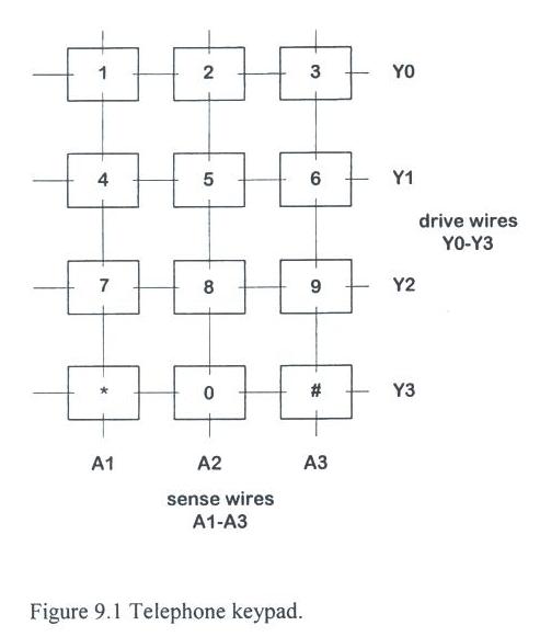
- It has buttons for 0-9 as well as for the asterisk and pound sign arranged in the usual 3 coulumns and 4 rows.
- Behind the button assembly is a printed circuit board which has 7 wires running rhrough it.
- A picture of a printed circuit board is shown in Fig. 9.2.

- Four of the wires run essentially horizontally and each of the wires runs beneath all three buttons in
a particular row.
- We will call those 4 wires the drive wires. The other 3 wires, called the
sense wires, run vertidally.
- Each wire goes underneath all 4 buttons in a particular coumn.
- Thus, each button has a unique pair (one drive and one sense) of wires underneath it.
- These wires do not normally make contact with each other, but are placed closely together in the inter-digitated
pattern shown in fig. 9.2.
- Each button is connected to a conducting post which is normally situated just avove the PC board.
- When a button is pressed, the conducting post touches the printed circuit board and the one sense wire and
one drive wire under that particular button are electronically "connected" together.
- For example, when you press the "5" button, sires A2 and Y1 become connected until the button is released.
- All other wires remain open(unconnected).
E. New Hardware
- There are a number of new components required for this lab.
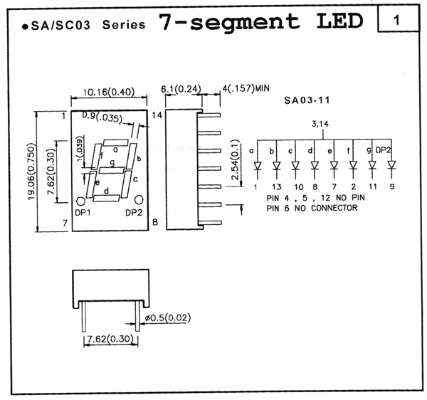
- The layout for the 7-segment LED is shown in Fig. 9.3.
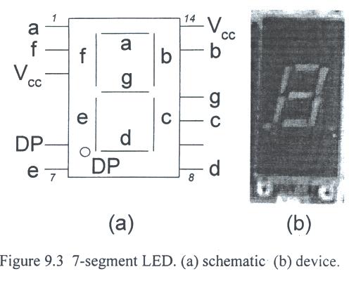
- Each of the seven thin segments and the decimal point(DP) is a separate LED.
- Each LED has a voltage drop of about 1 volt and required a current of about
10 mA when lit.
- The top LED is labeled "a", and the other LEDs are labeled consecutively going clockwise around the outside and
- ending with the middle LED "g". The LEDs are arranged on a plastic case which resembles a 14 pin DIP package.
- Three of the pins (#4. 5, and 12)are missing and one pin(#6) has no connection.
- The electridal connedtions for the LED display that we will use are given in Fig. 9.4.
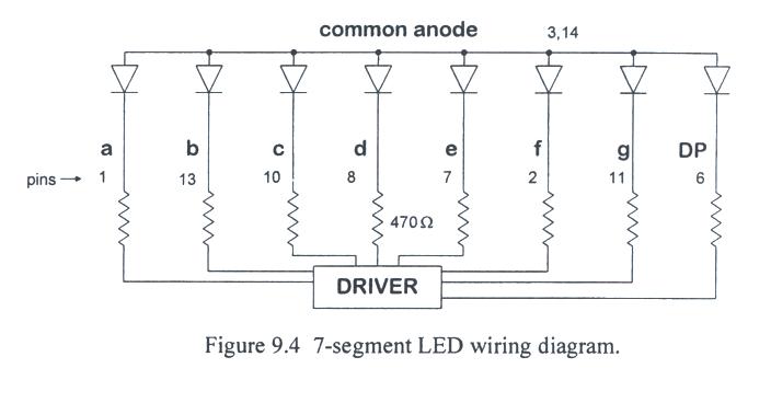
Other 7-segment LED.
- It is called a common anode arrangement because all of the diode anodes are connecdted to either pin 3 or pin 14
(and you will connect those pins together during the lab).
- Each cathode is connected to a separate pin.
- For normal operatrion, the anodes are all tied to 5 volts and each cathode is connected to a TTL "driver"
by a small resistance.
- The LED is turned on with a driver output of zero(i.e., the are "active low").
- The driver that we will use to activate the LED display is a 7446 and called a
BCD-to-7-segment display decoder/driver.
- The 7446 has open collector outputs and will not work unless it is porperly connected to
the display. The pin connections and the generic interface to the display are shown in Fig. 9.5.
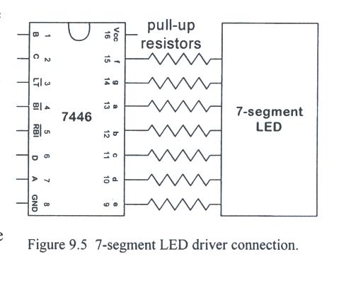
- The binary number to be displayed is encoded on the inputs as DCBA (i.e., D is the most significan digits).
- The chip decodes the number to activate the proper LED segments.
- For example, if the input is 3, then the outputs "e" and "f" will be high (off), but a-d and g will be low (on).
- The results for the LED outputs when the numbers 10-15 are input are not important
(*because those input combinations should not occur), but can be found in the on-line TI Data Book.
- The driver has a number of useful control inputs.
- The input (LT)' : Lamp Test, (RBI)' Ripple Blanking Input, (BI)'/(RBO)': Blanking Input/Ripple Blanking Output.
- The 7432 has four 2-input OR gates and the pin diagram is given in
Appendix C.
- The 74162 is a synchronous divide-by-10 counter. Its pin configuaration is identical to that of the 74163,
which we have discussed before, and the operation of the two counters is very similar.
- The 74162 simply counts 0-9.
- The 7475 is a 16 pin 4 bit binary D-latch and is generally used to
temporarily store information.
- The inputs are labeled 1D-4D and both the outputs and their complments are available on this 16-pin chip.
- Because of pin limitations, latches 1 and 2 are controlled by the same enable signal and latches 3 and 4 are
controlled by the other enable signal.
- The 74138 is an active-low 3-line to 8-line demultiplexer whose
pin connections are given in Appendex C.
- There are three control lsignals (G1, G2A, G2B) which can ber used to force all of the outputs high.
- They are useful for combining chips to get decoders with more than 8-lines,
but are not necessary for this lab.
- To disable the controls simply tie G1 to Vcc and tie G2A and G2B to ground.
- The input binary number is CBA (A is the LSB). The outputs are labeled Y0-Y7.
- The line that corresponds to the input number will be low and all the other lines will be high
(e.g., if CBA = 110, then Y6 will be low).
- The 74147 is a 16 pin 10-line to 4-line priority encoder.
- There are no control inputs for this device. The inputs and the outputs are both active low.
- There are acctually only 9 input lines: 1-9. If all inputs are high, it is assumed that the output should be
the number zero (zero corresponds to DCBA = 1111; A is the LSB).
- When more than two lines are low, the higher number takes precedence and that's the number that appears on
the output line.
F. Circuit Analysis

- There are no calculations that are required in order to design the circuit; rather this is an example of a seemingly
complex circuit which is much easier to understand if you subdivde it into modules and analyze them one by one.
- A sketch of the logic diagram that represents one realization of the circuit is give in Fig. 9.6.
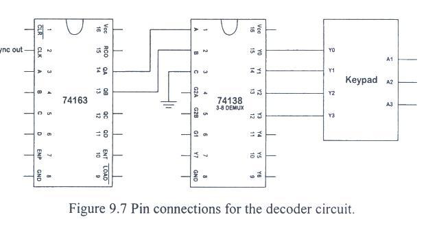
- An enlargement of the circuit module used to probe the keypad is shown in Fig. 9.7.
- Note that not all of the required connections are shown.
- The "sync out" from the function generator serves as the clock.
- The divide-by-16 counter is used to genreate the inputs to the demultiplexer.
- Because the keypad only has four drive wires, only half the output lines are used and the MSB (C) is grounded.
- The ideal signals into and out of the demultiplexer are shown in Fig. 9.8.
- The key point is that the drive wires are pulled low one at a time in a continuous cycle.
- When a key is depressed, one of the sense lines will be connected to one of the drive lines and will
go low repeartedly 1/4 of the time.
- If the sense wires are wired so that they are high when no button in the corresponding column is pressed,
then the button depressed is uniquely identified by the drive/sense wire pair that simultaneously goes low.
- The sense wires are connected to Vcc through small resistors to achieve the default value.

- The next module is the encoder, which needs to produce a number between 0-9. There are two possible sets of input wires.
- The first set utilizes the counter outputs QA and QB and the three sense wires.
- The second possiblility is to use the four drive wires and the three sense wires.
- Recall that the 74147 uses active low inputs.
- Since we are looking for combinations of sense and drive wires that are simultaneously low, we use a
set of 2-input OR gates, each connected to a unique drive/sense wire pair.
- Thus, at most, one of the OR gate outputs will ever be low.
- There are two minor problems with this particular encoder.
- First, a zero output on the encoder either means that the zero key is depressed or that no key has been depressed.
- The second problem is that even when 1-9 has been depressed, the encoder output is still zero 75% of the time.
- The second problem is solved by placing the D-latches betgween the encoder and the display driver.
- The first problem is solved with proper gating of the clock. The 3-input NAND gate will force the D-latch
"clocks" to be zero, which is the "hold" state, unless one of the keys has been pressed.
- There are many other possible ways to do the encoding and the clock gating; extera credit may be given for novel approaches.
Helpful Hints
- The Vcc and ground connections are not standard on the 7475. Be careful!
- Never EVER push more than one button on the keypad at a time.
- This lab is fairly long in that it has lots of components and many connections.
Be well prepared for class, check the wiring very carefulluy, and build and test the circuit in steps (modules).
Laboratory 9 Description
Objective:
- To build a circuit which senses input from a telephone keypad, decodes the input, and displays the digit
that was selected on a 7-segment LED.
Available Hardware:
TTL component boxes - see Appendix G.
Other components: 12 button telephone keypad 7-segment common anode LED
Pre-lab preparation:
Part I - 7 segment LED check
- Familiarize yourself with the operation of the keypad, the 7-segment LED, and the other
new components.
- Draw the logic and wiring diagram for a circuit that sequentially displays the numbers 0 - 9.
I.e., use a divide-by-10 counter as the input to a BCD to 7-segment decoder/driver, which in turn is connected
to a common-anode 7-segment LED via resistors.
Part II - telephone keypad circuit
- Draw the logic and wiring diagrams for each of the following subsystems(The subsystems may be drawn separately or all together on one page...)
- The circuit which generates the input signal to the telephone keypad. (Use a counter driven by "sync out" and a demultiplexer.)
- The circuit which decodes the signal from the keypad. This circuit uses the 7 lines from the keypad as input(the 4 "probe" wires and the 3 "sense" wires) and produces 9-10 output lines, at most one of which is active low at any given time.
- The circuit that encodes the output from the previous circuit to the correct BCD number.
- The circuit which holds and displays the BCD number on a 7-segment LED.
Part III - alternative decoder desigh
Part IV - alternative telephone keypad circuit design
- Design a display circuit where the LED blanks (is dark) any time no key is pressed.
Experimental Procedure:
DO NOT AT ANY POINT BEFORE, OR AFTER THE LAB DEPRESS MORE THAN ONE KEY AT A TIME ON THE KEYPAD!!!!
During this experiment, be certain that you:
- Ask the TA questions regarding any procedures about which you are uncertain.
- Turn off all power supplies any time that you make any change to the circuit.
- Do NOT apply more that 5 V to the circuit at any time.
- Arrange your circuit components neatly and in a logical order.
- Compare your breadboards carefully with your circuit diagrams before applying power to the circuit.
- Complete the following tasks:
Part I - 7 segment LED check
- Construct the circuit which uses the divide-by-10 counter to cycle a 7-segment LED.
Use the sync out from the function generator set to 1.5 Hz to drive the counter.
Have your lab TA verify that the circuit functions properly.
Part II - telepjone keypad dircuit - for "m" use the last digit of the current year(i.e., tor the year 2003, m=3)
- Remove the divide-by-10 counter and construct the circuit which sends pulsles to the
keypad. Set the function generator for a 20 kHz signal. Use the logic
analyzer to record the input signals to (2 channels) and output signals from (4 channels) the
demux. Also display the "sense" output from the keypad (3 channels) and when an m is
depressed. (Print the result.)
- Construct circuits 3.2 & 3.3 from the pre-lab section which translates the output from
the keypad into a BCE number. Use the logic analyzer to display (and print) the input to
(9 channels) and the output from (4 channels) the encoder when a m is depressed.
- Connect the output to the LED driver (via the latch circuit) and record the LED
response to the keys on the keypad. Have your TA verify that circuit works properly.
Part III
Part IV
- Modify your circuit so that athe LED blanks (is dark) any time no key is presed. Have your TA verify that the circuit works properly.
Post-lab analysis:
Generate a lab report following the sample report available in Appendix A. Mention any
difficulties encountered during the lab. Describe any results that were unexpected and try
to accoundt for the origin of these results(i.e. explain what happened). In ADDITION, answer
the following questions:
Part I - 7 segment LED check
Part II - telephone keypad dircuit
- What numbers reulted when you pressed the * and # keys in
4 above?
- Could you get the keypad operation to malfunction by varying the way you depressed the keys? If so, what do you think happened?
- Did you observe any glitches on any of the signals? If so, where? What do you think was the origin of the glitches and how could they be elimnated?
- What is the typical output voltage accross the LED segments?
- What is the typical delay time of the 7475 latch?
Part III