B. Background Reading
(Thevenin's theorem and Norton's theorem).
C. Definitions
- D/A converter - digital-to-analog converter: a circuit that has a number of digital inputs (which must be approximately either zero volts or VCC) and has a single output whose voltage is proportional to the number "represented" by digital inputs.
D. Laboratory Equipment
- DMM's will be used to measure resistances and DC voltage; oscilloscopes will be used for AC signals.
- There is only one meter in the lab that can be used to measure capacitance and inductance.
- The LC meter is a sophisticated machine that can measure a number of ideal and non-ideal
properties of inductors and capacitors.
- It is also an expensive, sensitive device that can be easily damaged if you are not careful.
- The most important rule of use is to ALWAYS DISCHARGE a capacitor before connecting it to
the LC meter.
- A capacitor is discharged by connecting the two terminals tightly and holding them together for a while.
- To operate the meter, follow the instructions on the card which slides out from undernath the LC meter.
- Basically, you just connect the component, select the desired measurement and wait for the result.
E. New Hardware
- The capacitors that we will use do not always have a simple identification scheme like resistors do.
- They also come in a wide variety of sizes, shapes, tolerances, and types that can be read about in a
number of places.
- You can use the LC meter to accurately measure the capacitance value.
- Still, we will use mostly electrolytic and ceramic capacitors in this lab.
- The electrolytic capacitors come in small cylindrical cans and usually have their capacitances printed
on them in microfarads.
- There are usually three numbers printed on a ceramic capacitor: N1N2N3.
- The capacitance value is given by C = N1N2 x 10N3 pf.
- They can also just have the value printed in microfarads. When in doubt, use the LC meter.
- Another complication is that some of the capacitors are polarized.
- These capacitors usually have a plus sign beside one terminal and a minus sign near the other.
- Polarized capacitors should be placed in circuits so that the plus terminal is always at higher potential than the minus terimal.
- These capacitors are generally made from materials that allow a large capacitance in a small volume but can sustain an electric field only in one diredction.
- These capacitors are normally used to "filter" out high frequency noise and to store energy for DC power supplies.
- You can safely apply AC signals with peak voltages well below the maximum rated voltage for the capacitor, but applying sustained potential in the opposite direction can redcuce the lifetime of the capacitor or even destroy it.
- Electrolytic capacitors are perhaps the most common polarized capacitors.
F. Circuit Analysis
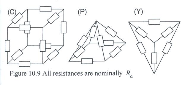
- The first circuit we will analyze is the resistive cube shown in Fig. 10.1a.
- The resistors are all assumed to have the same resistance, but are labled so that we can
keep track of their locations in the analysis.
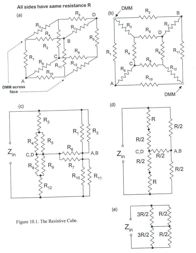
- Let's calculate the impedance across one of the faces of the cube. Say we connect one side
of a DMM to the node which connects R1-R3 and the other side to the node
containing R10-R12.
- None of the resistors are simply connected in series or parallel, so we need to use general
analysis methods (e.g., mesh analysis) or we need to look for sysmmetries which can be exploited
to simplify the analysis.
- Note that due to the finite tolerances of real resistances, no exact symmetries exist.
- However, if the variation in resistances is small, we might expect the final impedances of the
real and ideal cubes to be close.
- In the lab you will quantify this argument.
- The cube can actually be drawn as a two-dimensional circuit as indicated in Fig. 10.1b.
- The DMM connections are at the upper-left and lower-right corners.
- Notice that if we were to draw a line through R3 and R12 and then flip
the circuit about that line, the circuit looks identical.
- Therefore, the potentials at points A and B must be identical and the potentials at C and D
must be equal.
- Consequently, we can connect wires between A and B and between C and D without changing the
circuit operation.
- The resultant circuit is shown in Fig. 10.1c. The five pairs of resistors that are now in
parallel have been simplified in Fig. 10.1d. This operation leaves two pairs of resitors in series.
- Notice that the half of the circuit above the horizontal (R/2) reesistor is identical to
the part of the circuit below the horizontal resistor.
- Thus, the potential on either side of the horizontal resistance will be identical (and 1/2 of
any potential applied across the cube face) and we can either remove that resistor altogether, or
connect a wire getween points A and C.
- The resulting simplification is shown in Fug. 10.1e. Performing the final parallel and series combinations results in a final input impedance of Zin = 3R/4. Note that the valitity of the final simplification (connecting nodes A and C) can actually be seen in Fig. 10.1b.
- The second circuit to consider is the infinite R-R ladder shown in Fig. 10.2a. How do we calculate the
input impedance?
- If the ladder had a finite number of stages, we would simply start at the rightmost end and repetitively
use series and parallel combinations to reduce the circuit to a single imput impedance.
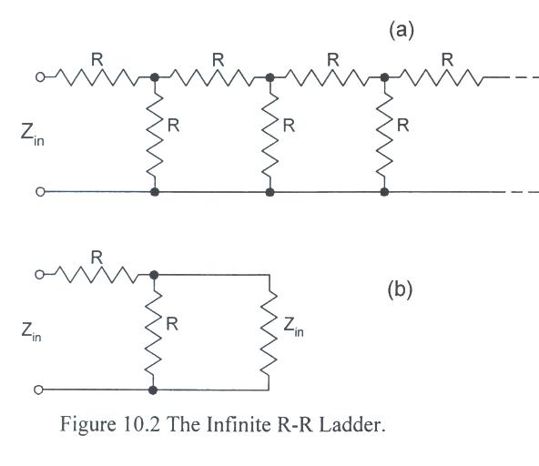
- However, none of the resistors in the infinite ladder are in series or parallel.
- Since there are an infinite number of stages, adding or deleting a a stage won't change the impdedance.
- This is illustrated in Fig. 10.2b, where we have replaced the infinite ladder with an equivalent impedance
Zin (on the right) and then added another stage.
- Thus, the input impedance must be equal to R plus the parallel combination of R and Zin:
- Zin = R + R||Zin = R + RZin/(R + Zin)
- Solving for Zin, we get
- Z2in - RZin - R2 = 0
- or
- Zin = R(1 +/- 51/2)/2.
- The negative solution is unphysical since the resistance must be positive, so
- Zin = R(1 + 51/2)/2 (= 1.618R).
- How many stages are required to approximate an infinite ladder?
(Hint: Zin,n = R + R||Zin,n-1, and Zin,1 = 2R)- How do resistor tolerances affect the result? These are questions to be answered by the lab.
- Zin = R + R||Zin = R + RZin/(R + Zin)
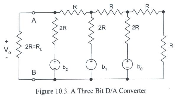
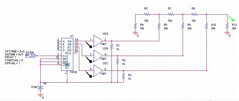
- A three-bit D/A converter is shown in Fig. 10.3. The supplies b0 - b2 are either zero volts or Vcc.
- They could be realized manually via SPDT switches connected to ground on one side and Vcc
on the other.
- We interpret the binary number as b2b1b0. In other words, the number 5 is
realized by setting b2 and b0 to Vcc and b1 to ground.
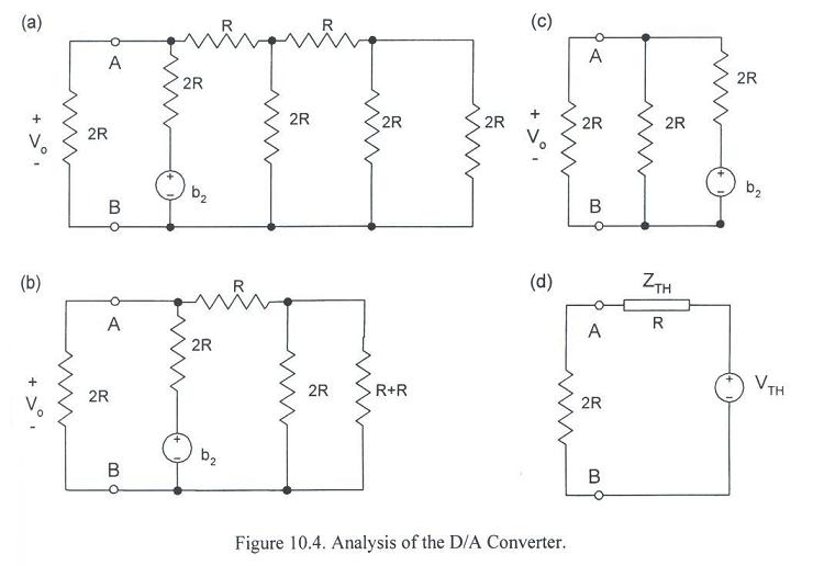
- Our interest in this example is to calculate the Thevenin equivalent nonideal source for the case where
b0 and b1 are grounded.
- The sequence of parallel and series simplifications is shown in Fig. 10.4a-c.
- To find the input impedance in Fig. 10.4d, we set the source to zero to get ZTh = R.
- The Thevenin equivalent voltage is the open circuit voltage drop across A-B, which is seen to be
VTH = b2/2 because the relevant circuit is a resistor-divider with 2R on both legs.
- Can you draw a Thevenin equivalent nonideal source when all three power supplies are present?
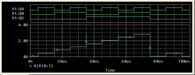
[Hint: V0 = (4b2 + 2b1 + b0)/12; See pages 122-124 in (M/L)] (See PSpice simulation; schematic and plot.)
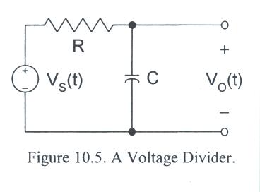
- Now consider the circuit in Fig. 10.5. How can we calculate and measure the Thevenin equivalent circuit parameters?
- The calculation is straightforward. The open circuit voltage comes from the voltage divider equation for phasors:
- V0/Vs = Zc/(Zc + ZR) = 1/(1 + jwRC)
- where Zc(=1/jwC) and ZR are the capacitor and resistor impedances, respectively, and w is the source frequency in radians/sec.
- The equivalent input impedance simply consists of a parallel combination of a resistor and capacitor:
- ZTH = ZR||Zc = R/(1 + jwRC).
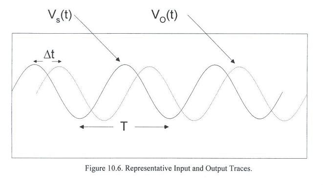
- Now, how do we measure the parameters? We can measure both the open-circuit output voltage and the source voltage on the oscilloscope.
- Figure 10.6 shows how a typical set of traces may look. What we can measure is the difference in amplitude of the two signals and the phase difference.
- To compare with thory, it is convenient to rewrite the normalized output voltage in exponential form:
- V0/Vs = e-jqT/[1 + (wRC)2]1/2 = |V0/Vs| e-jqT
- where
- qT = tan-1(wRC),
- and then to convert the answer to the time domain.
- If you define the source phase angle to be zero, then we have in the time domain:
- vs(t) = Vm cos(wt)
- and
- vo(t) = Vm|Vo/Vs|cos(wt - qT).
- The measurements can easily be used to get the Thevenin equivalent voltage source as follows.
- The measured amplitude is simply equal to the output voltage amplitude. If the peak output voltage lags the peak input voltage in time by Dt, the relative phase shift is
- qT = 2pDt/T
- where T = 2p/w is the signal period and qT is given in radians. If the peak output leads the peak soource voltage, then Dt and qT are negative.
- To get the Thevenin equivalent impedance, we need to measure the short-circuit current.
- In the absence of a current probe, the best thing to do is to short the output and measure the voltage across resistor.
- Dividing by the resistance, which can be accurately measured with a DMM, we can determine the short circuit current.
- Then we can put it in exponential polar form and use the fact that ZTH = Voc/Isc.
- There are two important observations that we can make here. First, given the frequency, the theoretical equations for the magnitude and phase contain two variables: R and C.
- Therefore, the two measurements can be used to estimate the product RC (but not R & C separately, because they always appear as the product!).
- Second, the Thevenin equivalent circuit varies with frequency. At low frequency, the equivalent voltage nearly equals the source voltage, but at high frequency the equivalent voltage is greatly reduuced.
- Also, the low frequency equivalent source has the same phase as the input source, but at high frequency the phase is advanced by 90o.
- This circuit is an example of a simple (first-order) low -pass filter.
- As a final example, consider the circuit in Fig. 10.7. It is much more complicated to theoretically calculate the Thevenin equivalent source for this situation.
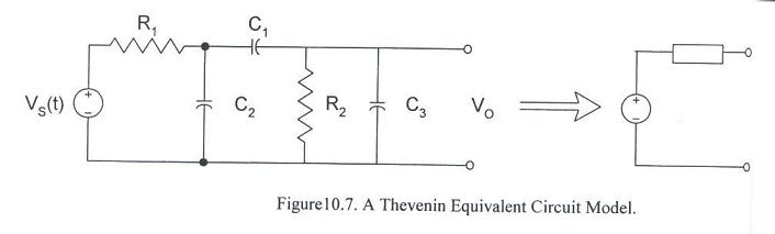
- However, the measurement would be exactly the same if we had a current probe.
- It's a little trickier to do the short circuit measurement, but with the LC meter (and the frequency) the procedure is still staightforward.
- Still, can you qualitatively analyze the circuit at low and high frequencies to estimate the performance?
- V0/Vs = Zc/(Zc + ZR) = 1/(1 + jwRC)
Helpful Hints
- To plot the phase of a voltage of current in an AC sweep in PSpice, just enclose the quantity in parentheses and place a "p" in front for phase (or use the p() function in the probe "trace add" menu). For example, to plot the phase at the second terminal of capacitor C1, on the "trace command" line in the "add traces" dialog box in PROBE, type: "p(V(C1:2))". Warning! If you want to plot simultaneously amplitude and phase, you should do it on two separate plots. Click on the "plot" drop down menu and then "add plot". An "SEL>>" appears to the left of the :"active plot, which is the plot that traces will be aded to with the "add trace" command. To make another plot active, simply move the mouse to that polt and click the left mouse button. Note: this phase funcytion is only for AC simulations; it doesn't make sense for transient simulations, and thus won't work.
-
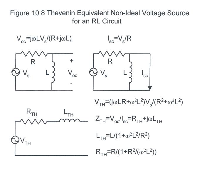
- Figure 10.8 below shows the calculation for a Thevenin Equivalent Nonideal Voltage Source for an RL series circuit at a specific frequency. The calculation for an RC circuit is quite similar.
Laboratory 7 Description
Objective:
Available Hardware:
| Lab | R0 (kW) | m | n | p | t |
|---|---|---|---|---|---|
| A | 1 | 1 | 2 | 5 | Y |
| B | 2 | 3 | 1 | 3 | P |
| C | 2 | 1 | 2 | 6 | C |
| D | 2 | 1 | 2 | 6 | Y |
| E | 1 | 3 | 5 | 3 | P |
| F | 1 | 1 | 3 | 3 | C |
| G | 1 | 1 | 3 | 3 | Y |
| H | 1 | 2 | 3 | 5 | P |
| I | 2 | 3 | 1 | 5 | C |
| J | 1 | 2 | 3 | 6 | Y |
| K | 1 | 1 | 2 | 5 | P |
| L | 1 | 3 | 1 | 6 | C |
Pre-lab preparation:
Part I - Thevenin equivalent resistances
- Calculate the Thevenin equivalent resistance across the side, face, and diagonal of the cube shown in Fig. 10.9C.
- Calculate the Thevenin equivalent resistance across the pyramid base sides and diagonals shown in Fig. 10.9P.
- Calculate the Thevenin equivalent resistance of the infinite ladder circuit shown in Fig. 10.10.
Calculate the resistance if the ladder has only 2, 3, or 4 mR0 stages. (Each stage has two resistors: mR0
and nR0.)
Part II - Thevenin equivalent of D/A
- Calculate the equivalent nonideal voltage source for the 3-stage D/A converter shown in Fig. 10.3
when the input is p.
- Use PSpice to calculate the open-circuit voltage and the input impedance for the 3-stage D/A
converter shown in Fig. 10.3 when the input is p.
Part III - Thevenin equivalent of a low-pass filter
- Simulate the circuit shown in Fig. 10.11 and plot the input and output voltages versus time at
100 Hz, 1kHz, and 10 kHz. Compute the Thevenin equivalent nonideal voltage sources for the circuit at those three
frequencies. Set the input voltage to 4 V p-p.
Part IV - Thevenin equivalent of a 3-capacitor circuit
- Simulate the circuit shown in Fig. 10.12 and plot the output voltage (magnitude and phase) from 1 Hz to 10 kHz. Compute the Thevenin equivalent nonideal voltage source for the circuit at 300 Hz.
Experimental Procedure:
During this experiment, be certain that you:- Ask the TA questions regarding any procedures about which you are uncertain.
- Turn off all power supplies any time that you make any change to the circuit.
- Do NOT apply more that 5 V to the circuit at any time.
- Arrange your circuit components neatly and in a logical order.
- Compare your breadboards carefully with your circuit diagrams before applying power to the circuit.
- Complete the following tasks:
Part I - Thevenin equivalent resistances
Part II - Thevenin equivalent of D/A
Part III - Thevenin equivalent of a low-pass filter
Part IV - Thevenin equivalent of a 3-capacitor circuit
Post-lab analysis:
- Generate a lab report following the sample report available in Appendix A. Mention any difficulties encountered during the lab. Describe any results that were unexpected and try to account for the origin of these results (i.e. explain what happened). In ADDITION, answer the following questions:
Part I - Thevenin equivalent resistances
Part II - Thevenin equivalent of D/A
Part III - Thevenin equivalent of a low-pass filter
Part IV - Thevenin equivalent of a 3-capacitor circuit

- Generate a lab report following the sample report available in Appendix A. Mention any difficulties encountered during the lab. Describe any results that were unexpected and try to account for the origin of these results (i.e. explain what happened). In ADDITION, answer the following questions: