ENEE 206
March 30, 2004
Laboratory 13 - Rectifier Circuits
A. Lab Goals
- In this lab you will learn about the operation of diodes, and characterize half-wave and
full-wave rectifier circuits both with and withourt filtering.
- You will also learn about zener diodes and design, construct, and test a simple regulated
"power supply."
B. Background Reading
- Read about diodes and diode circuits (Section 7.6 in (M/L)).
- Read also about PSpice simulations with diodes in Section 7.7 of M/L. Note that a simulation
of a full-wave rectifier bridge is discussed on pages 284-286.
C. Definitions
- Cutin voltage - the threshold forward-bias voltage above which a diode readily conducts
current.
- Diodes - a two-terminal non-reciprocal device that is made of two types of semiconductor
material and allows current to flow in only one direction.
- Voltage ripple - The difference between the minimum and maximum voltages across the output
load in one-period (assuming steady-state operation). It can be found on a typical digital
oscilloscope via a peak-to-peak voltage measurement of the signal. Voltage ripple is an important
measure of the quality of power supplies (the smaller, the better of course!).
- Rectifier bridge - an arrangement of four diodes which enables full rectification of
an AC signal. i.e., if the voltage input to the bridge is a sine wave, the output voltage is the
absolute value of the sine wave.
- Zener diode - a diode which is designed to operate reversed-biased and is often used as a
crude voltage regulator or as part of a more complicated DC "power supply".
D. Laboratory Equipment
- An oscilloscope will be used for all measurements. A variable transformer may be used to
produce the 60 Hz AC signal.
- The transformer is encased in a plastic box. One side of the transformer plugs into a
wall-plug outlet.
- The turns ratio is such that the other side of the transformer has a maximum voltage of 6.3 V rms.
- The knob on the box is attached to a variable contact on the transformer and can be
used to reduce the voltage below the maximum.
- The voltage output is connected to two banana jacks and is floating
(neither side is attached to graound).
E. New Hardware
- Standard diodes and zener diodes are both used for the first time in this lab. The symbol for
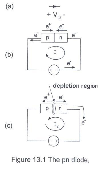
a diode is shown in Fig. 13.1a.
- The diode is made up of two types of semiconductor material: p-type and n-type.
The connection to the p-side is called the anode; that of the n-side is the cathode.
- Details of how diodes work are discussed in a later course (ENEE 302).
- Basically, like wires, electrons carry current in the n-type material. Howeer,
positive charges (holes) carry the current in the p-type device.
- When a positive votage is applied to the p-side of the diode, current flows from the
p-side to n-side.
At the jnction, the electrons and holes "recombine" to continue the current flow (Fig. 13.1b).
This configuration is called "forward bias" operation.
- However, when a positive voltage is applied to the n-side of the diode, current "tries" to flow in the
opposite direction, but that causes holes and electrons to flow away from the p-n junction, leaving
a "depletion" region devoid of free-charge.
- This depletion region inhibits current flow (Fig. 13.1c). This configuration is called
"reverse bias."
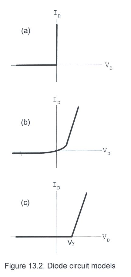
- Three models for the V-I terminal relationship for a diode are given in Fig. 13.2.
- The ideal model is shown in Fig. 13.2a. For any reverse bias, the current flow is zero.
- When any forward bias is applied, the voltage drop across the diode is zero, and any
current can be made to flow.
- Thus, an ideal diode behaves like a switch: reverse-biased diodes are open switches and
forward-biased diodes are closed switches.
- The terninal relationship for a real diode is given by (see Fig. 13.2b):
ID = I0(eVD/nVT - 1)
where I0 is the reverse saturation current, n is a material-dependent constant
(between 1 and 2), and VT = kBT/q where kB is Boltzmann's
constant, and T is the diode temperature in oK. Usually I0 is a few
microamps.
- A simplified model for a diode, known as the piecewise linear model, is shown in Fig. 13.2c.
The diode current is zero for all voltages up to the cutin voltage,
Vg.
- We will use silicon diodes, for which the cutin voltage is about 0.6 V. Above the cutin
voltage, the V-I relationship is a straight line whose slope represents the forward bulk
resistance of the diode.
- Diodes can be damaged in a number of ways. If a diode were placed directly across a power
supply without any other elements in series and the supply voltage were well aboove 0.6 V,
the diode would draw a large current, overheat, and burn out.
- If too large of a reverse bias is applied, the diode can "break down" and large currents
will flow, again damaging the diode.
- The reverse break-down voltage depends on how the diode is constructed. We will use a
1N4007 diode which has a high breakdown voltage near 1000 V.
- Some diodes can actually be fabricated to allow a reverse breakdown without damaging
the diode (below a certain current level). When this happens, it is called "zener"
breakdown and the diode is called a zener diode.
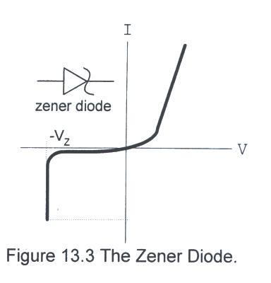
- The symbol for a zener diode and the V-I terminal relationship are given in Fig. 13.3.
Notice that the slope of the V-I curve at the zener breakdown voltage Vz is
very sharp.
- This means that a zener diode can be used to maintain a nearly constant voltage over
a wide range of currents.
- For this reason, zener diodes are often used in voltage regularion circuits for constant
dc power supplies.
F. Circuit Analysis
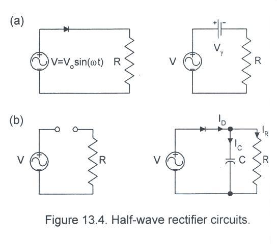
- Consider the unfiltered half-wave rectifier circuit shown in Fig. 13.4a. The source voltgage
is just a sine wave as shown in Fig. 13.5a.
- When the source voltage is positive, the applied voltage across the diode is positive.
Therefore, according to the ideal model, the diode is "on" and can be replaced by a short.
- Thus, the voltage across the load resistor equals the source voltage. During the times
when the source voltage is negative, the diode is "off" and can be replaced by the open circuit
shown in Fig. 13.4b.
- Thus, no current flows through R, by Ohm's Law the output voltage is zero, and the source
voltage appears across the reverse-biased diode.
- Because the negative voltages are not transferred to the load resistance but the
positive half of the wave is, this cicuit is called a half-wave rectifier.
- For a diode circuit where you are not certain whether a diode is "on" or "off", one
approach to solving the problem is to assume that the diode is off and replace it with an open.
Solve the resultant problem and check the voltage across the diode.
- If it is negative, the solution is fine. If posivtive, replace the diode with a short and
resolve the problem. If originally you assume the diode is "on", check the current in the
resultant solution. If the current flows in the right direction you have the correct solution.
Otherwise, replace it with an open and solve it again.
- If there are many diodes in a circuit, this approach is impractical. If an educated guess
does not quickly yield correct results, one can always use PSpice.
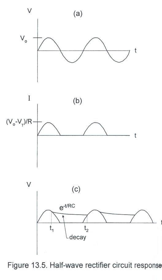
- If the source voltage is relatively small, it may not be possible to neglect the cutin voltage. In this case, the diode is "on" only when V > Vg, and the model for the "on" diode is a battery as shown in Fig. 13.4c. The resultant current through the resistor is shown in Fig. 13.5b.
- While the half-wave rectifier circuit converts an AC signal with zero average voltage to
a signal with a positive average voltage, the waveform is still far from a DC signal.
- We will now investigate a sequence of circuits designed to reduce the ripple and make the
output voltage closer to DC.
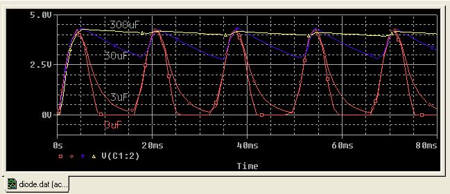
- The simplest improvement comes from placing a "filter" capacitor in parallel with the output
load as shown in Fig. 13.4d.
- The basic idea is that when the source voltage is positive,
the capacitor will charge up, and when the voltage source is negative, the stored energy in the
capacitor will be used to supply power to the load.
- When the diode is "off" the output is a simple RC circuit which is characterized by an
exponetial voltage decay with a time constant t = RC.
- The output voltage signals with and without a filter capacitor are shown in Fig. 13.5c.
- The times when the diode turns on and off can be found from KVL and KCL.
Assuming the voltage source is given by v(t)=V0sin(wt), the
current through the ideal diode when "on" is (in phasor form):
ID = -jV0/Z = -jV0(1 + jwRC)/R
- so the diode current as a function of time is:
id(t) = (V0/R)[1 + (wRC)2]1/2
sin[wt + tan-1(wRC)].
- The times when the diode current is zero are given by
t1 = [p - tan-1(wRC)]/
w = (T/2)[1 - tan-1(wRC)/
p]
- where T is the period of the sine wave.
- If either the capacitor or the resistor is very small,
the cutoff time is T/2 and the circuit is essentially unfiltered.
- If RC is large,
t1 ~ T/4 and the diode cuts off near the maximum voltage. The time the diode turns
back on again is more complicated. The voltage on the capacitor while it is discharging is:
Vc(t) = V0
(wt1)e-(t-t1)/RC.
- When this voltage is equal to the source voltage again the diode will turn on. If that time
is denoted t2 > t1, we have:
Vc(t2) = V0
sin(wt1) e-(t2-t1)/RC =
V0 sin(wt2).
- We can rearrange these terms to get an implicit equation for t2:
e t1/RC cos(wt1) = e t2/RC cos(wt2).
- The relative voltage ripple is given by:
DV/V0(%) = |1 - cos(wt2)| x 100.
PSpice simulation of half-wave rectifier
- Now consider the full-wave unfiltered, bridge rectifier circuit shown in Fig. 13.6a.
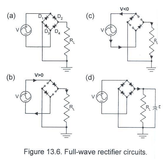
- Consider first the times when the AC voltage source is positive. Since the p-side of ideal diode
D2 is at the highest potential and the n-side of D3 is at the lowest potential, it is likely
those diodes are "on."
- If we assume the other two diodes are off, we arrive at the configuration shown in Fig. 13.6b. Note that
current will flow through D2, down through the resistor and then through D3.
- For this configuration D1 and D4 will be reversed biased as assumed. If the AC signal
is the usual sinusoidal shown in Fig. 13.7a, the resistor voltage during the positive source voltage intervals is shown
in Fig. 13.7b.

- When the source voltage is negative the diode roles are reversed and D1
and D4 are on, while D2 and D3 are off as shown in Fig. 13.6c.
- Even for this case the current flows down through the resistor so the source and load
voltages are 180o out of phase as indicated in Fig. 13.7c.
- The net output voltage is shown in Fig. 13.7d. Because this circuit is unfiltered, the
voltage ripple is 100%.
- However, the period of the output voltage has been cut in half, so when a filter capacitor
is added as in Fig. 13.6d, the ripple is greatly reduced as indicated in Fig. 13.7e.
- The analysis of this circuit is nearly identical to that of the half-wave filtered circuit
and is left to the reader.
- As a final circuit, consider the zener-regulated circuit shown in Fig. 13.8.
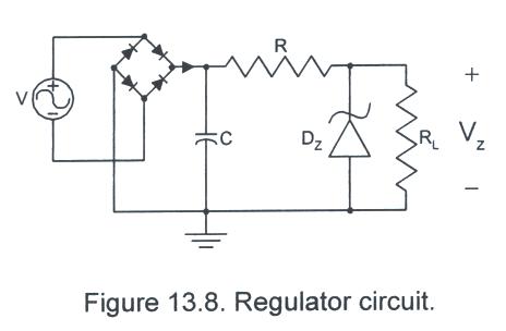
- It is similar to the filtered full-wave rectifier circuit except that the load resistor is
replaced by the combination of R, RL, and Dz.
- Assume that Dz is ideal, and that the voltage Vz across Dz
is constant as long as the (reverse) current through Dz is greater than zero.
- How can we choose R so that there is no ripple on the output voltage? Let's assume the load
resistor RL can vary from Rmin to infinity and that we choose the
capacitance C such that the voltage ripple on Vc is less than 10%.
- Then the minimum current through R is Imin =
[0.9(V0 - 2Vg) - Vz]/R.
- That current must be greater than Vz/Rmin if the zener is to be kept
regulating, so
R < Rmin[0.9(V0 - 2Vg)/Vz - 1].
- On the other hand, the zener diode power is limited (or it will overheat and burn out), so
the zener current Iz must be less than some Imax.
- This puts an lower bound on R, because when RL is infinite and Vc is
maximized, the zener current is
Iz = (V0 - 2Vg - Vz)/R <
Imax
- so
R > (V0 - 2Vg - Vz)/Imax
- For the sake of concreteness, lets plug in V0 = 10 V, Imax = 65 mA,
Rmin = 2 kW, and Vz = 5.3 V
(let Vg = 0.6 V), than we find 54 W
< R < 988 W, so there is considerable margin to pick R.
G. Helpful Hints
- In the full-wave rectifier circuits, the voltage source MUST BE floating. If you need
to measure both the source voltage and the output voltage simultaneously, on the oscilloscope,
you must be careful!
- You cannot place probe grounds in two different locations, if you do, most likely the
circuit will not work because it will "short out" part of the circuit.
- Instead, you must use the trace subtraction feature to measure the source voltag or
you can measure the source and output voltages at different times and store one of them in memory.
- WARNING!!! Unlike resistors, diodes are not reciprocal devices and the
direction the diode is placed in a circuit is very important.
- The usual way to denote the "n" side of a diode is with a band at the end of the
(cylindrical) housing. (Recall that current flows OUT of the "n" side)
- Make certain that you install all diodes correctly. Failure to do so could result
in the voltgae source shorting out *(and being damaged and in need of expensive repairs).
- Never place a diode directly across the terminals of the voltage source.
This may happen, for example, if you place a diode backwards in the rectifier bridge of a
full wave rectifier.
- The PSpice simulation of the full-wave rectifier bridge is discussed on pages 284-286
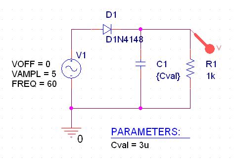
in Mayergoyz and Lawson. Also, to help with the aPSpice exampple called diode.sch from the web.
- The example has a filtered, half-wave rectifier circuit which is driven by a 5 V,
60 Hz AC sourcde(VSIN). The simulation is set up to do a transient analysis.
Take a careful look at the setup menus to see how this analysis should be run.
Additional information can be found in the 204 book and in the PSpice references (on the web).
- If when you click on the link you see a text file, you can copy text file and
save it on you computer as "diode.sch", or you can go back and click on the link with the
right mouse button and select "save link as" from the menu.
- There is a set of cursors that can be used in PROBE to "measure" the voltage or
cxurrent amplitude or phase at different points in the PSpice output plots.
- When you are in PROBE and you have one or more traces already plotted, go to the
TOOLS drop-down menu, then go to CURSOR and slide the mouse to lthe right and then click on
DISPLAY in the menu that appears. A box will appear on the screen that suyas "probe cursor"
and contains six numbers.
- To give the X coordinates (one for each cursor -usually time of frequency), two give
the Y coordinates (the measurements), Moving the mouse to a point on the c
screen and clicking the left mouse button will move one cursor to the trace at that X coordinate.
- Clicking the right mouse button will move one cursoe to the rrace at that X coordinate.
Clicking the right mouse button controls the other trace.
- You can also move the cursors with the arrow keys (use the shift key plus the arrow
keys for one of the cursors). If you want to change which trace is measured by the cursors,
move the mouse to the trace symbol to the right of the trace label
(*bottom, left-hand part of the screen) and click whichever mouse button corresponds to the
cursor that you wanmt to move (click both buttons to move both cursors to the new screen).
Read the valued you need in the probe cursor box.
See how to simulate a rectifier circuit with Capture CIS
Laboratory 13 Description - Rectifier circuits
Objective:
- To learn about diode operation and to characterize half-wave, full-wave, unfiltered, filtered,
and regulated rectifier circuits.
- In class, you will be told to do one of the following labs: 13A - 13D. Look at the table
below for the regulator voltage that corresponds to your lab. Do Lab 13A with VS = 8V.
| Lab | Zener | V1 | VS
|
|---|
| 13A | 1N753A | 6.2V | 6V
|
|---|
| 13B | 1N751A | 5.1V | 6V
|
|---|
| 13C | 1N749A | 4.3V | 5V
|
|---|
| 13D | 1N746A | 3.3V | 5V
|
|---|
Available Hardware:
- Analog component boxes - see Appendix G.
Pre-lab preparation:
Unless otherwise stated, asssume for the following circuits that there is a simple resitive load
R and and AC source with an amplitude of 5 V(rms).
Part I - Half-wave rectifier
s
- Draw wiring diagrams for an unfiltered, half-wave rectifier circuit.
- Draw the wiring diagram for a filtered, half-wave rectifier circuit.
- Simulate the filtered, half-wave rectifier in the previous step with PSpice for a
circuit with a 220 mF filter capacitor and a 1 kW
load resistor. Plot the output voltage for source frequencies of 50, 60, and 400 Hz and measure
the voltage ripple.
Part II - Full-wave rectifiers
- Draw the wiring diagram for an unfiltered, full-wave rectifier circuit.
- Draw the wiring diagram for a filtered, full-wave rectifier circuit.
- Simulate the filtered, full-wave rectifier in the previous step with PSpice for a circuit with a
220 mF filter capacitor and a 1 kW load resistor. Plot the
output voltage for source frequencies of 50, 60, and 400 Hz and measure the voltage ripple.
Part III - Zener regulator
- Draw the wiring diagram for a filtered, full-wave rectifier, with a V1:_____ zener diode regulator.
- Simulate the regulator circuit in the previous step with PS;pice. Choose a resistance
value R that keeps the zener diode regulating for the minimum load resistance of 2 kW and keeps the zener5 vcurrennt below 70 mA for all loads greater than 2
kW. Find the capaitance necessary to keep theripple below 1%
(on the output) when the load is 2 kW (using tiral and error with
PSpice is perfectly acceptable for this part). With these resistance and capacitance values, plot
the time dependdence of the output voltae for loads of 51 W and 2
kW. For a 51 W load, plot the output for a
source frequency of 50 Hz and 400 Hz. Assume the source voltage is VS
(Vrms): ______.
Part IV - clamping circuit
- Design a clamping circuit that will keep the output voltage a minimum of about 4 V. I.e. if
the output voltage is more than 4 volts, the clamping circuit does nothing, but if the output
voltage starts to fall below 4 volts, the clamping circuit "kicks in" and forces the output to
remain at 4 volts until it naturally rises above 4 volts again. Note that for the clamping circuit,
you only meed one diode amd one variable DC power supply.
- Use PSpice to simulate the circuit from the previous step. Connect an AC source to
the clamping circuit and a 1 kW load, and vary the peak amplitude of
the source from 0 - 10 V. Plot the voltage across the output load.
See clamp.pdf.
Experimental Procedure:
During this experiment, be certain that you:
- Ask the TA questions regarding any procedures about which you are uncertain.
- Turn off all power supplies any time that you make any change to the circuit.
- Arrange your circuit components neatly and in a logical order.
- Compare your breadboards carefully with your circuit diagrams before applying power to the circuit.
- Note: ONLY for step 6 below use the function generator as the source. For all other srtewps, use the 60 Hz vriable transformer in the black bos!!! Set rhe rms voltage of the ad source to t V.
- Complete the following tasks:
Part I - Half-wave rectifiers
- Construct the unfiltered half-wave rectifier with a 1 kW load resistor. Plot the input and output voltages. Reverse the diode direction and plot.
- Add a 220 mF filter capacitor. Measure the voltage ripple on
the output and plot input and output voltages.
- Repeat the measurement in the previous step with a source frequency of 50 Hz and 400 Hz.
Do not plot the input and output voltages - only measure the ripple.
Part II - Full-wave rectifiers
- Construct the unfiltered full-wave rectifier with a 1 kW load
resistor. Plot the input and output voltages. Note: You shopuld use two probes and waveform math (subtraction) to measure the input voltage.
- Add a 4.7mF capacitor. Measure the voltage ripple on the
output and plot input and output voltages.
- Replace the filter capacitor with a 220mF capacitor.
Measure the voltage ripple on lthe output and plot input and output vltages.
- Repeat the measurement in the previous step with a source frequency of 50 Hz and 400 Hz.
Do not plot the input and output voltages-only measure the ripple.
Part III - Zener regulator
- Beginning with the circuit from step (5) at 60 Hz, construct the filtered, regulated
rectifier circuit with a V1:_____ zener diode. Set the source voltage to Vs:____. Measure the
average voltage across the load and the voltage ripple for resistive loads of 51
W and 2 kW and for both a 220mF
filter capacitor and for the ccapacitor that you determined in pre-lab Part III(step #8)
simulation(4 meassurements total). Plot the input and output voltages for the simulated filter
capacitor value and a 2 kW load.
Part IV - Clamping circuit
- Build the clamping circuit designed in pre-lab Part IV.9 and plot the input and oujtput
voltages over a non-trivial range of values. For example, use an AC source at 60 Hz, attach a
1 kW load, and measure the load voltage as the input amplitude is
varied from 1 V up to some "interesting" value.
Post-lab analysis:
Generate a lab report following the sample report available in Appendix A. Mention any
difficulties encountered during the lab. Describe any results that were unexpected and try
to account for the origin of these results(i.e. explain what happened). In ADDITION, answer
the following questions/instructions:
Part I - Half-wave rectifiers
- ....
- ....
Part II - Full-wave rectifiers
- ....
- ....
- ....
Part III - Zener regulator
- ....
- ....
Part IV - Clamping circuit
- ....
Laboratory 8 Pre-lab Questions - Rectifier circuits
- ....
- ....
- ....
- ....
- ....
- ....
- ....